As current and new display technologies ramp up pixel resolution, pixel measurement techniques are keeping pace to ensure consistent quality.
JESSY HOSKEN AND DOUG KREYSAR, RADIANT VISION SYSTEMS
In 2017, Clay Bavor, then vice president of Google’s AR/VR division, spoke for all AR/VR device makers when he said, “We need pixels. Way, way more pixels.”1 The display industry has more than risen to that challenge in the subsequent years, offering new products today — such as 4K, 8K, and ultra-HD screens — that offer many more pixels per inch (PPI). Pixel sizes have been shrinking along with pixel pitch (the distance between pixels) to deliver increasingly high-resolution displays.
However, these sharper displays have also created the need for new display metrology systems that can measure
much smaller, more densely packed pixels. The need to detect defects and ensure a uniform display appearance is as important as ever to maintain product yields and to meet customer expectations. This demand applies to all types of display devices and embedded displays — from smartphones, televisions, and computer screens to the dashboard displays in automobiles.
Quality challenges
The emergence of emissive display technologies based on OLEDs and micro-LEDs has only increased display measurement challenges. These display technologies are called “emissive” because each pixel acts as its own emissive element, individually powered and emitting its own light. Mini-LEDs can also be used as individual emitters, but more commonly they are used as a backlight behind LCD display panels in the same way LEDs have been used for decades.
Because the pixels in OLED and micro-LED displays are individual emitters, they can exhibit broad variability in luminance and color output from pixel to pixel (Figure 1). This variability manifests as nonuniformity and defects — also known as “mura,” from the Japanese word for unevenness or irregularity — in the display image (Figure 2). Such mura results in low yield of acceptable displays, rejection of expensive components, or costly rework.
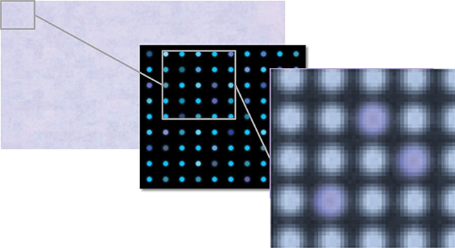
Figure 1. An example of nonuniform output for individual pixels on an emissive display. In aggregate, this nonuniform output results in an uneven screen appearance, called mura, to human viewers. Courtesy of Radiant Vision Systems.
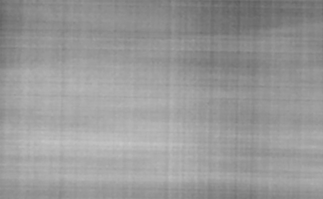
Figure 2. An OLED display with line mura defects. Courtesy of Radiant Vision Systems.
Automated visual inspection of displays using imaging photometers and colorimeters is the established solution to identify defects and measure uniformity for displays of all kinds. These systems can provide quantitative pass-fail results within the fast cycle times that are necessary for mass production and commercialization.
However, ensuring measurement
accuracy for qualification and correction at the pixel level becomes more challenging as pixels become smaller, more numerous, and closer together. The latest OLED smartphone displays contain
anywhere from 2 million to more than
4 million pixels per display (with 3 or 4× the number of subpixels). Further, pixel pitch for these displays ranges from
400 PPI to more than 500 PPI, and a few have even topped 1000 PPI.
For an emissive display, it is necessary
to measure not only each pixel but also
the display’s individual subpixels. Subpixel inspection allows calibration of displays for uniformity by identifying, measuring, and correcting the luminance output of each pixel, thereby producing displays of entirely uniform appearance. This process — referred to as pixel uniformity correction, or the demura process — relies on the accuracy of luminance and chromaticity measurement to calculate accurate correction coefficients for each pixel.
The demura process
To correct display uniformity, the demura process employs four distinct steps. The first step is pixel registration, a method of dynamically locating and setting a region of interest (ROI) around each pixel in the measurement area.
Measurement is step two. Each subpixel in the ROI is then measured to calculate luminance values at each pixel coordinate location. Ideally, measurements are made with a high-resolution imaging colorimeter to ensure that
measurement values for each subpixel are as accurate as possible. The method
involves displaying test images on screen to allow the colorimeter to target subpixels of each color set. This enables
computation of measurements and correction factors for each set. For example, a green test image can be shown to illuminate all green subpixels. An imaging colorimeter then measures and records the output of each individual green subpixel. This approach is then repeated for all the primary colors and, usually, white-light emissions.
Calculation, step three, follows measurement. The measurement data from each pixel’s coordinate position is loaded into a coefficient calculator, which employs test analysis software to calculate correction factors that can be applied to normalize luminance and chromaticity
discrepancies between pixels in the display.
The final, and fourth, step is correction. Correction factors are applied to the electrical input of each individual subpixel at each pixel location, using an external control system.
These four steps ensure that brightness and color will be accurate and uniform across the entire display, including at all gray levels. When this pixel uniformity correction process is applied to a finished OLED or micro-LED display, there is a significant improvement in the product’s
visual quality. The net effect of the
demura process is that displays that would otherwise have failed quality inspection without electronic compensation will
now be able to pass. Demura methods, therefore, help to reduce wasted manufacturing materials, while improving cost
efficiency and increasing production yields.
Accurate pixel-level measurement
An effective demura process depends, above all, on accurate pixel and subpixel measurement. But today’s OLED and micro-LED pixels can be measured in mere microns. Discerning these tiny
elements requires an imaging device
with sufficient resolution to measure each individual pixel of the display under measurement (Figure 3).
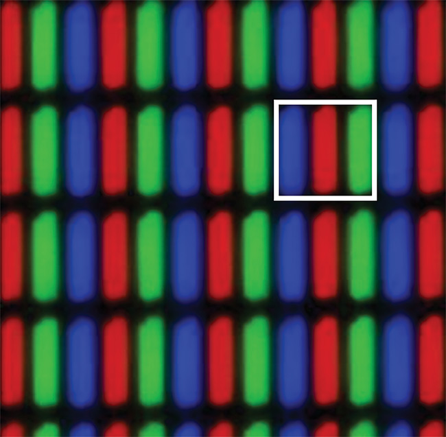
Figure 3. A close-up of an OLED display. Each pixel (white square) is composed of one red, one green, and one blue subpixel. Displays may also include white subpixels. Courtesy of Radiant Vision Systems
Applying more sensor pixels per display pixel increases the granularity of data acquired by the imaging system and allows for more accurate subpixel measurement. To increase the accuracy and repeatability of pixel-level measurement values, image-based measurement systems must maximize both the number of sensor pixels across each display
pixel (pixel registration) and the data captured by each sensor pixel (pixel measurement).
But achieving this ratio of sensor pixels to display pixels is becoming more
challenging as the overall resolutions of
today’s displays increase. Measuring a display using multiple images can increase the effective imaging resolution per pixel, but this also increases takt time, or the time it takes to complete a measurement for each display. Thus, capturing single-image measurements with maximum resolution is important for correcting a display at the low takt times needed for efficient high-volume production processes.
Demura process challenges
Registration involves setting an ROI centered on each pixel to define the area around each display pixel in the measurement image. This technique was originally patented for the purpose of measuring individual LED pixels in large-format outdoor screens, for which measurements are performed over extended periods and multi-image measurement of a single
display is common to optimize image
sensor resolution per display pixel.
The ROI can be set as a uniform grid aligned to the image sensor array. Each ROI, in this case, is aligned to the center of an image sensor pixel, not necessarily to the exact center of a display pixel. This approach works well for multi-image, resolution-optimized measurement scenarios. Because so many sensor pixels cover each display pixel, the ROI does not need to precisely align to the display pixel center — though aligning the ROI to an image sensor pixel often achieves display pixel alignment anyway.
When it comes to quality control of smaller displays — such as those used in smartphones, watches, or microdisplays — manufacturers do not have the luxury of multi-image measurement. They instead need single-image measurement to meet production speeds. This approach reduces the available sensor resolution per display pixel and makes it less likely that the centers of sensor and display pixels will align (Figure 4). This reduces the ROI’s ability to precisely cover and isolate each display pixel for measurement.
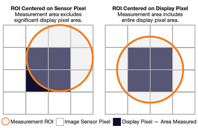
Figure 4. When it comes to quality control of smaller displays, manufacturers need to apply single-image measurement methods to meet production speeds. This approach can make it more challenging to precisely align the centers of sensor and display pixels (left). The region of interest (ROI) for each display pixel (orange circle) should be aligned to the center of an image sensor pixel that ideally, though not necessarily, aligns with the exact center of a display pixel (right). Courtesy of Radiant Vision Systems.
The demura process also depends on accurate measurement of registered pixels. This makes it important to maximize the amount of data acquired by each of the image sensor pixels, which becomes challenging in scenarios in which fewer sensor pixels can be applied to measure a single display pixel. It is hard to exactly measure the quantity and quality of the light produced by a single display pixel when the light is captured by sensor pixels collecting data inside and outside the bounds of the display pixel’s ROI. Accuracy demands that only sensor pixels within the ROI of a target display pixel are used to obtain the true value for that pixel.
Pixel-level measurement accuracy
Several approaches can be used to solve these registration and measurement challenges for high-resolution emissive displays.
Use a high-resolution imaging system. Although many imaging photometers and colorimeters can be found in the 6- to
12-MP sensor range (6 to 12 million pixels), cameras on the market today can offer resolutions as high as 45, 61, or even 151 MP. Not all sensor pixels are created equal, however. They are distinguished by factors such as their comparative pixel size and well depth, which can affect the sensor performance beyond its resolution. But, in general, high-resolution imaging devices bring many more sensor pixels to bear on the measurement of individual display pixels.
Use image magnification. Equipping an imaging colorimeter with a microscope lens can increase the granularity of pixel measurements. A microscope lens provides objective measurement with, for example, 5× or 10× zoom capability. This allows detailed measurement of
each individual emissive element (Figure 5).
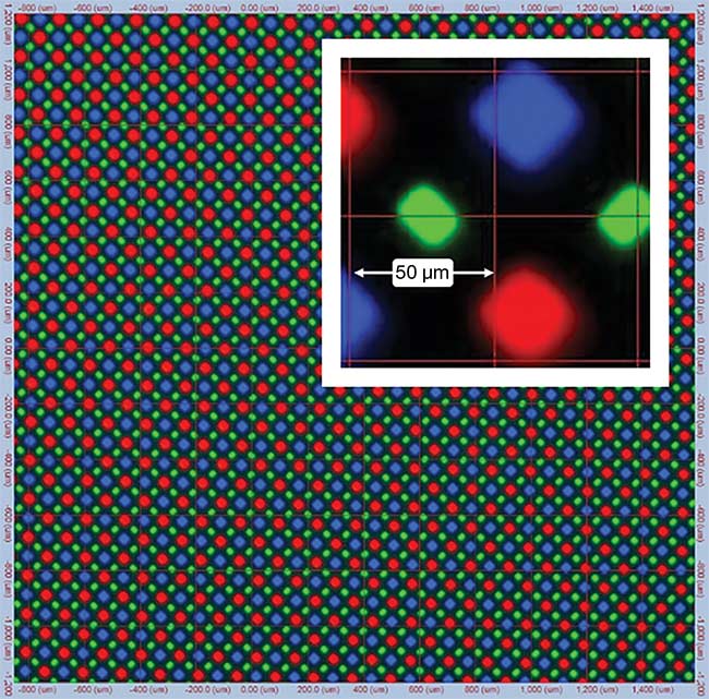
Figure 5. The subpixel measurement taken by a 29-MP imaging colorimeter is magnified by a microscope lens to show a 50-µm distance at 10× zoom (inset). Coupling an imaging colorimeter with a microscope lens can increase the granularity of pixel measurements and allow detailed measurement of each individual emissive element. Courtesy of Radiant Vision Systems.
Coupling a high-resolution imaging system with a microscope lens enables the capture of every display pixel over multiple sensor pixels for increased measurement precision. This type of system is effective for the evaluation of display subpixels and the characterization of individual micro-LEDs.
Use software methods. Independent of camera resolution or magnification, methods exist to increase the accuracy of pixel measurement based on sophisticated software algorithms. Two software methods that have been proven to significantly improve an imaging system’s ability to isolate and measure increasingly small subpixels in increasingly high-resolution displays are the patented Spaced Pixel and Fractional Pixel methods.
Using one or more of the three approaches provided above has enabled demura processes to keep pace with the increasing resolutions of OLED, micro-LED, and other advanced displays. With the successful application of demura processes, emissive display components at the wafer, panel, and assembly stages of production can be brought up to quality standards that enable them to be shipped to customers (Figure 6).
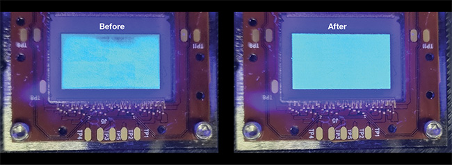
Figure 6. Variable luminance creates a nonuniform appearance in a 0.7-in. micro-LED panel (Full HD, 1920 × 1080) with LEDs measuring 2 µm and a pixel pitch of 8 µm (left). The same micro-LED display with uniform luminance after measurement and correction using a 29-MP imaging photometer equipped with a microscope lens and supported by software applying demura algorithms (right). Courtesy of Jasper Display Corp.
Conclusion
For OLED, micro-LED, and other high-resolution displays, subpixel measurement methods have enabled the calibration of display uniformity by identifying, measuring, and correcting the luminance output of individual pixels to produce displays of entirely uniform appearance. Single-image measurement is important for correcting displays at a pace that meets the need for short takt times. By
applying hardware, optics, and/or software approaches, display manufacturers can increase the accuracy of the values used to correct the appearance of their displays, as well as to increase yields and ensure customer satisfaction.
Meet the authors
Jessy Hosken, a product manager at Radiant Vision Systems, helps oversee product life cycles, including guiding, documenting,
and communicating product developments.
She holds a bachelor’s degree in physics; email: [email protected].
Doug Kreysar is CEO of Radiant Vision Systems, where he leads the company’s
strategy and business operations in North America and Asia. Kreysar holds a bachelor’s degree in physics and a master’s degree in applied physics. He is the author of multiple technical papers, a regular speaker for industry organizations, and he holds eight U.S. patents; email: [email protected].
References
1. C. Bavor (May 23, 2017). Enabling rich and immersive experiences in virtual and augmented reality. Proc. Society for Information Display, Display Week 2017 Symposium, Los Angeles, Calif.