Progress and Promise
Dr. G. Ferris Lipscomb and Marc Stiller
Integrated circuits have revolutionized electronics and have begun to make good on their promise to do
the same for photonics, but challenges remain.
Since the beginning of the most recent boom in the optical fiber
industry, component vendors have introduced many technologies, among them planar
optical integration, in which optical circuits are constructed out of waveguides
fabricated on silicon wafers. The manufacturing process for these optical circuits
uses the tools and techniques developed by the semiconductor industry, which was
itself transformed 30 years ago by the integrated circuit chip.
However, while planar optical integration has
made substantial progress, both in technology and in market acceptance, the wavelength
of a telecommunications photon is 10,000 times bigger than an electron, providing
a fundamental limit to the amount of integration that can be achieved. That said,
the state of the art is not at all close to these fundamental limits, and a lot
of headroom is left to exploit the technology.
Key measures of its developmental status
are performance and level of integration. Equipment vendors demand components that
push the boundaries of achievable performance. There is no place for subspecification
parts in current or next-generation systems. But planar lightwave circuits must
also deliver lower cost and size through increased integration.
The most commercially advanced optical
integration technology — silica-on-silicon — has demonstrated that it
can provide both performance and the benefits of integration. For example, 40-channel
variable optical attenuator multiplexers replace 40 discrete attenuators, 39 filters
and their associated piece parts.
Another example is arrayed waveguide
gratings, which perform multiplexing and demultiplexing functions in parallel on
one chip. Over the last two years, they have gained a significant percentage of
the total multiplexer/demultiplexer market because a single chip in a single package
can perform either function for 40 channels in parallel. Also, the production costs
for high-channel-count devices are much lower than for competing technologies.
To achieve performance that is equivalent
to a 40-channel arrayed waveguide grating, thin-film filters and fiber Bragg gratings
would require 39 designs, production runs and packaging operations.
Meanwhile, 80-channel arrayed waveguide
gratings have been introduced to the market, and 256-channel devices have been demonstrated
in the laboratory.
Initially, arrayed waveguide gratings
did not provide the same performance as the other technologies, and most believed
that discrete parts had an intrinsic performance advantage over integrated devices.
However, intense development to improve their performance has made them equivalent
to competitive technologies in all major parameters.
Because arrayed waveguide gratings
process all channels in parallel, they have had a significant advantage in insertion
loss for high-channel-count applications. Essentially, insertion loss is the same
for 4-, 40- or 80-channel devices; the discrete variety, however, is used in series,
and the losses accumulate.
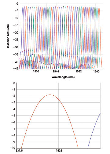
Figure 1. Already low,
the insertion losses for arrayed waveguide gratings continue to drop. In
these plots
of the transmission spectrum of an ultralow-loss 40-channel,
100-GHz-spaced Gaussian
arrayed waveguide grating, the insertion loss for the center channels at
the ITU
grid point is around 2 dB, and all 40 channels have insertion losses
lower than
3 dB.
Performance in isolation
Another key performance parameter is isolation,
which is a measure of how much light from an unwanted channel leaks into the passband
of an active channel. For discrete filters, such as thin-film filters and fiber
Bragg gratings, isolation is determined by nearest-neighbor crosstalk — the
amount of light that leaks into a channel from its immediate neighbors.
Integrated devices, including arrayed
waveguide gratings, offer an extra level of isolation. Instead of dropping away
as it does in a thin-film filter, the transmission curve of an arrayed waveguide
grating levels off in the noise floor because these devices process channels in
parallel, with all channels in one chip. Light scattered or lost because of imperfections
in one channel might scatter into any other.
Eighteen months ago, a noise floor
around 35 dB was considered good, and adjacent channel isolation for both arrayed
waveguide gratings and thin-film filters was around 25 dB. However, totaling up
the contributed noise floor from the gratings’ other 37 channels dropped its
cumulative isolation to only 19 dB. By applying strict process control and focused
improvement programs, top vendors of the devices now achieve adjacent-channel isolations
of 30 dB and noise floors lower than 50 dB.
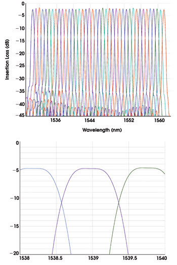
Figure 2. Ultralow-loss
wide-band, or “flat top,” arrayed waveguide gratings have
demonstrated insertion losses between 4 and 5 dB. Similar progress has
been made
in reducing polarization-dependent loss. Typical loss for a top-tier
arrayed waveguide
grating is now 0.1 to 0.2 dB measured across the passband.
Spectral plots show low noise floor
(Figures 1 and 2). When all channels are added together, the noise floor is not
significant, and the total isolation of an arrayed waveguide grating is dominated
by adjacent-channel isolation. These devices now exhibit total cumulative isolation
as good as that from the best thin-film filters and fiber Bragg gratings.
Arrayed waveguide gratings also carry
significant advantages over discrete devices in regard to chromatic dispersion.
Because they do not have multiple reflections and all of the wavelengths have virtually
the same optical path, chromatic dispersion is very low (Figure 3). In counterpoint,
multiple reflections from thin-film filters and fiber Bragg gratings create different
path lengths for different wavelengths, resulting in significant pulse spreading.
A typical thin-film filter can have ±30 to 40 ps/nm across the passband and
up to 60 ps/nm of change over the passband.
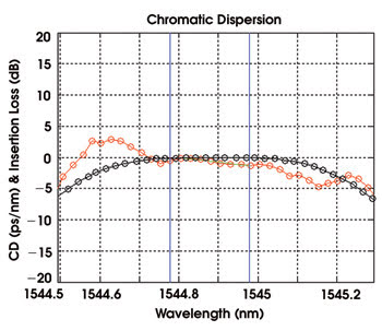
Figure 3. Chromatic dispersion, measured across the passband of an
arrayed waveguide grating, is very low and very flat. The black curve represents
the passband shape, and the red curve represents chromatic dispersion.
Planar integration’s potential
extends beyond multiplexing/demultiplexing applications. Next-generation networks
require active components that enable systems with automatic and dynamic adaptability.
Emerging dynamic planar light chip products use the thermo-optic effect to alter
the index of the silica, delivering dynamic control. Companies such as NEL in Saddle
Brook, N.J., and Lightwave Microsystems are shipping 40-channel variable optical
attenuator multiplexers based on this technology (Figure 4).
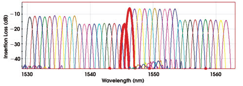
Figure 4. Each of the 40 output channels of a variable optical attenuator multiplexer can
be set to any arbitrary attenuation. The dynamic range of the device is 10 dB. The
minimum insertion loss at 0-dB attenuation is approximately 6 dB.
These devices not only lower production
costs, but also reduce 79 separate packages to one. Also, use of discrete attenuators
requires that each be spliced or connected and that the fibers be properly routed
to assemble the final subsystem. Although integration can streamline this configuration,
a 40-channel variable optical attenuator multiplexer is considerably more complex
than a simple passive optical component (Figure 5). It also must match the performance
of discrete implementations.
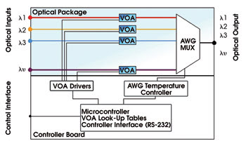
Figure 5. In a variable optical attenuator multiplexer, passive functions
performed by the arrayed waveguide multiplexing filter are combined with active
functions performed by the variable optical attenuators. Besides combining these
functions, the module integrates electronic controls to adjust the attenuators,
stabilize the waveguide temperature and communicate with the system.
A challenge for designers of planar
lightwave chips is polarization-dependent loss. Such loss is very low for discrete
mechanical variable optical attenuators because the light remains inside the fiber.
The engineering of planar devices, however, must keep polarization-dependent loss
low, and this has been successful (Figure 6).
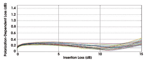 Figure 6. The overall performance of variable
optical attenuator multiplexers is such that major equipment companies are designing
them into systems. This plot of polarization-dependent loss vs. insertion loss shows
that all 40 channels of an array of attenuators have losses below 0.4 dB, out to
the specification limit of 10-dB attenuation.
Figure 6. The overall performance of variable
optical attenuator multiplexers is such that major equipment companies are designing
them into systems. This plot of polarization-dependent loss vs. insertion loss shows
that all 40 channels of an array of attenuators have losses below 0.4 dB, out to
the specification limit of 10-dB attenuation.
Thermo-optic elements can perform other
active functions, such as that of the dynamic gain-flattening filters, which are
entering the commercial market. NEL offers an 8 x 8 thermo-optic cross connect and
arrays of eight 2 x 2 thermo-optic switches. Several companies are developing integrated
versions of reconfigurable optical add/drop multiplexers based on planar lightwave
circuits, thermo-optic switches and arrayed waveguide gratings.
Things to come
At their present stage, planar integrated optics
diverge significantly from the analogy of semiconductor integrated circuits. In
simplified form, electronic chips obtain their power from the integration of millions
of transistor gates that basically perform the same function in the same material.
Optical networks require many different functions, all performed by different optimized
materials. Therefore, planar integration of optics will more closely resemble microwave
hybrids, where many smaller-scale integrated components are assembled on a common
platform. The silica-on-silicon planar lightwave circuit is a strong candidate for
an optical integration platform.
In parallel with the large-scale planar
integration product development described above, a completely separate set of planar
lightwave circuits has emerged, including integrated fiber optic transceivers pioneered
by Lucent, Nortel, NEL and Bookham Technology. Sometimes called a silicon optical
bench, a small planar lightwave chip offers a platform on which to mount laser and
photodetector chips, and waveguides are used to interconnect these optical elements.
In some cases, active chips are prepositioned, using pick-and-place tools, and techniques
such as solder bump bonding provide the precise positioning between separate optical
elements. Input and output fibers are positioned using V-grooves etched into the
silicon substrate. Other optical elements, such as coarse wavelength division multiplexing
filters, and electronic chips, such as laser drivers, also can be added.
Currently, transceiver modules are
relatively small, such as might fit into a dual in-line package, whereas arrayed
waveguide grating/variable optical attenuator chips are several centimeters on a
side. While the scale of these is different for these two applications, planar lightwave
chips are made with the same tools and can be matched to one another.
The markets are large for large- and
small-scale planar lightwave chips, but the promise of optical integration will
be fulfilled when these two technologies are unified in a single platform to provide
both active and passive optical functions in proximity with electronic control.
It will be neither monolithic nor hybrid, but a combination. Each optical function
can be performed in an optimized material system, but will also be capable of integration
with dissimilar technologies through the platform.
We are just beginning to explore the
potential of such integration, and the capability of the planar lightwave circuit
industry will be built up over time.
Meet the authors
G. Ferris Lipscomb is vice president of marketing
at Lightwave Microsystems in San Jose, Calif. Marc Stiller is director of product
marketing.