
Plasmonic Nanowire Shows Promise as Photonic Circuit
A new kind of nanowire efficiently guides both light and electricity.
A team from the University of Rochester and the Swiss Federal Institute of Technology developed a basic photonic integrated circuit consisting of a silver nanowire and a single-layer flake of molybdenum disulfide (MoS2). The concept could translate to computer chips capable of transporting digital information at the speed of light.
MoS2 is made up of layers that are weakly bonded to each other, so they can be easily separated. In bulk MoS2, electrons and photons interact as they would in traditional semiconductors like silicon and gallium arsenide. As MoS2 is reduced to thinner and thinner layers, the transfer of energy between electrons and photons becomes more efficient.
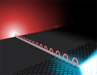
Far-field photons excite silver nanowire plasmons. The plasmons are absorbed in the MoS2, creating excitons that subsequently decay and convert back into propagating photons. Courtesy of Michael Osadciw/University of Rochester.
In a study, the researchers used a laser to excite plasmons at the surface of the nanowire. Examining the system with scanning confocal fluorescence microscopy and spectroscopy, they found that the MoS2 flake at the far end of the wire generated strong light emission.
In the other direction, as the excited electrons relaxed, they were collected by the wire and converted back into plasmons, which emitted light of the same wavelength.
Typically, about a third of the remaining energy would be lost for every few microns that the plasmons traveled along the wire. “It was surprising to see that enough energy was left after the round-trip,” said Rochester graduate researcher and lead study author Kenneth Goodfellow.
“We have found that there is pronounced nanoscale light-matter interaction between plasmons and atomically thin material that can be exploited for nanophotonic integrated circuits,” said Dr. Nick Vamivakas, assistant professor of quantum optics and quantum physics at the University of Rochester.
The structure of the MoS2 energy bandgap gives it desirable photonic properties. As the material’s layer count decreases, it transitions from an indirect to direct bandgap, which allows electrons to easily move between energy bands by releasing photons.
The researchers said the next step is to demonstrate their primitive circuit with light-emitting diodes.
The research was published in Optica (doi: 10.1364/optica.1.000149).
For more information, visit www.rochester.edu.
Published: September 2014