Compiled by Photonics Spectra staff
Until recently, plasmonic properties have been limited to nanostructures
with interfaces between noble metals and dielectrics. But now researchers have discovered
that plasmonic properties also can be achieved in quantum dots.
Scientists at the US Department of Energy (DoE)’s Lawrence
Berkeley National Laboratory have demonstrated well-defined localized surface plasmon
resonances that arise from p-type carriers in vacancy-doped semiconductor quantum
dots. These should allow for plasmonic sensing and manipulation of solid-state processes
in single nanocrystals, researchers say. The quantum dots could open up possibilities
for light harvesting, nonlinear optics and quantum information processing.
Plasmonics describes the phenomenon in which the confinement of
light in dimensions smaller than the wavelength of photons in free space makes it
possible to match the different length scales associated with photonics and electronics
in a single nanoscale device.
The key to plasmonic properties is when the oscillation frequency
between the plasmons and the incident photons matches, a phenomenon known as localized
surface plasmon resonance (LSPR). Conventional scientific wisdom has held that LSPR
requires a metal nanostructure, where the conduction electrons are not strongly
attached to individual atoms or molecules. The Berkeley Lab scientists have proved
that this is not the case.
“Our study represents a paradigm shift from metal nanoplasmonics,
as we’ve shown that, in principle, any nanostructure can exhibit LSPR, so
long as the interface has an appreciable number of free charge carriers, either
electrons or holes,” said Prashant Jain, a member of the research group. “By
demonstrating LSPR in doped quantum dots, we’ve extended the range of candidate
materials for plasmonics to include semiconductors, and we’ve also merged
the field of plasmonic nanostructures, which exhibit tunable photonic properties,
with the field of quantum dots, which exhibit tunable electronic properties.”
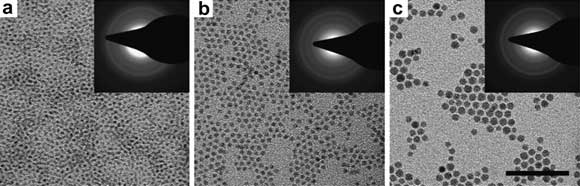
Transmission electron micrographs
(inset) showing the electron diffraction patterns of three quantum dot samples with
an average size of (a) 2.4 nm, (b) 3.6 nm and (c) 5.8 nm. Courtesy of the Paul Alivisatos
group.
The group made its quantum dots from the semiconductor copper
sulfide, a material known to support numerous copper-deficient stoichiometries.
Initially, the copper sulfide nanocrystals were synthesized using a common hot injection
method. Although this yielded nanocrystals that were intrinsically self-doped with
p-type charge carriers, there was no control over the amount of charge vacancies
or carriers.
The investigators used a room-temperature ion exchange method
to synthesize the copper sulfide nanocrystals, which froze them into a relatively
vacancy free state. They then doped them in a controlled manner using common chemical
oxidants, Jain said. This enabled the group to achieve LSPR in the near-infrared
range of the electromagnetic spectrum.
Jain envisions quantum dots as being integrated into a variety
of future film- and chip-based photonic devices that can be actively switched or
controlled, and also being applied to optical applications such as in vivo imaging.
And there is the potential for applications in solar photovoltaics, artificial synthesis,
and quantum communication and computation devices.
Supported by the DoE Office of Science, the work was published
online April 10, 2011, in Nature Materials (doi: 10.1038/nmat3004).