As planar polymer waveguide technology has evolved, it has enabled a multitude of highly functional optical sensor applications.
NIKOLAUS FLÖRY AND THOMAS HUGHES, VARIO-OPTICS
The worldwide sensor market is growing rapidly with the establishment and growth of new applications, such as medical devices that leverage noninvasive optical sensors, and environmental monitoring, which is gaining importance due to a rise in the need for both indoor and outdoor air quality measurements.
Courtesy of vario-optics.
The growing range of applications is also widening the requirements for optical sensors. Their increasing deployment in smart devices and Internet of Things applications, for example, is driving the need for low-cost, compact, yet powerful sensors. For a long time, the demand for smaller form factors was satisfied by designs built upon electronic or microelectromechanical systems (MEMS). However, MEMS design principles face limitations in terms of sensitivity and specificity — both qualities in which
sensors built on optical principles excel.
Up until recently, though, most optical sensor systems were based on free-space or fiber-based components, rendering them too bulky and costly to be deployed in large numbers, unlike their electronic and mechanical counterparts.
This gap is now being closed by a growing field of integrated photonic technologies.
With continuing advancements in photonic integrated circuits (PICs) and the availability of high-throughput semiconductor-like fabrication methods, it is only a matter of time until photonic sensors will revolutionize the sensing market.
The rise of photonic sensors
The principles behind integrated photonics are simple. Rather than guiding a beam of light through free space via discrete elements such as lenses and
mirrors, integrated photonics takes advantage of total internal reflection at the interface between two media exhibiting different refractive indices. This way, a waveguide core — a narrow strip of high-index material surrounded by a low-index “cladding” material — is able to guide light within a customized planar photonic circuit to the desired output and sensing spots.
The advantages of integrated photonics are manifold. Many free-space optical elements, such as beamsplitters, mirrors, and so on, have counterpart building blocks within integrated photonic circuits. Hence, a sensor based on optical waveguides typically comprises far fewer discrete components. This not only circumvents laborious assembly and alignment processes, it also allows high-volume reproduction of photonic chips.
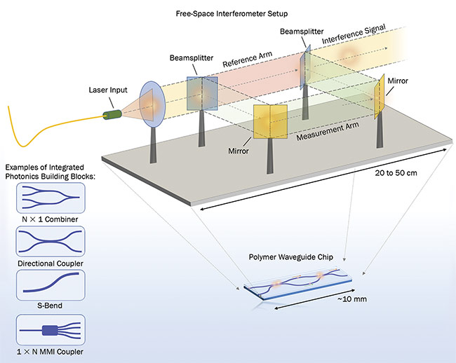
Photonic miniaturization enabled by planar waveguide chips allow much more compact devices, such as on-chip interferometers. MMI: multimode interference. Courtesy of vario-optics.
Moreover, having fewer discrete optical elements makes alignment less problematic, and the device’s smaller size permits a far more stable optical path versus free-space architectures. These qualities make an integrated system far less sensitive to unwanted vibrations, temperature changes, or other environmental disturbances.
Integrated photonics platforms
Within the last 10 years, a variety of planar waveguide platforms have emerged. They are distinguished by the materials systems used and their respective properties, which impart certain limitations and advantages to each of them. The range of platforms spans from highly integrated silicon photonics to silicon nitride (SiN) and lithium niobate (LiNbO3) platforms, to glass and polymer waveguides and others.
For a long time, the development of most of these platforms was driven by applications from the telecommunications sector. Today, as PIC manufacturing costs drop and photonics technologies mature, they have provided a broader basis for novel smart optical sensor applications. This holds true, in particular, for those PIC platforms that can be integrated easily with existing fiber components, such as glass or polymer waveguides.
Polymers have long been considered an exotic materials system in the engineering world, due to the vast range of chemical structures and intrinsic properties these materials encompass. However, in recent years, polymer optics have gained more attention as a result of their manufacturing simplicity.
A large percentage of modern smartphones, for example, feature camera lenses made of polymer material rather than glass, due to the easier fabrication of polymers, as well as their robustness and lower cost.
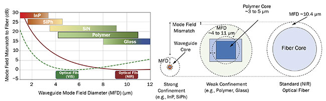
Several photonic integration platforms have emerged over the past decade. Defined either by materials systems or the platform’s respective properties, they exhibit a wide range of optical properties. Courtesy of vario-optics.
Similarly, polymer waveguides are an attractive alternative to other highly integrated PIC platforms, such as silicon photonics or indium phosphide (InP). While typical PIC chips have dimensions
of a few millimeters per side and are processed on wafers with a fixed size, polymer waveguides can be manufactured in sizeable quantities on large panels by means of UV photolithography. Making use of the tooling and standards from the printed circuit board (PCB) industry provides an easier, more common process flow and cuts production costs.
In terms of performance and handling, polymers offer one particular advantage that is especially relevant to sensor applications. In contrast to many other PIC platforms, polymer waveguides share roughly the same dimensions and optical properties with standard optical glass
fibers, which makes their combination with commonly used pigtailed laser sources or detector modules comparatively more straightforward.
Polymer waveguides can either accommodate multimode (with core dimensions typically between 30 and 500 µm) or single-mode (with core dimensions between 2 and 5 µm) operation. In both cases, they are easily compatible with the corresponding optical fiber type.
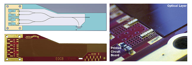
An example of an electro-optical circuit board (EOCB) for a sensor device The optical
design can be incorporated into the electrical layout. Courtesy of vario-optics.
For example, the mode field diameter
of single-mode optical fibers can be matched precisely with polymer waveguides in different wavelength ranges (e.g., between 4 and 6 µm in the visible, and between 9 and 10 µm in the near-infrared), allowing very efficient fiber-chip coupling.
Various use cases
Due to their versatility, the use cases of polymer waveguides in photonic sensors are manifold. Two main functionalities that stand out are light guiding and interferometry.
In light-guiding applications, optical waveguides serve the simple purpose of combining light from multiple LEDs, laser diodes, or other light sources into one common channel — a waveguide or fiber — and subsequently guiding it to specific measurement points.
One particular feature of polymer waveguides is that their optical layer can be smoothly integrated with electrical PCBs, thereby resulting in a so-called electro-optical circuit board (EOCB).
The optical layout of a photonic waveguide circuit is typically based on custom- or predesigned photonic building blocks, such as splitters, couplers, or other optical elements that are optimized and adapted using common optical design software — often Zemax for multimode operation or Lumerical for single-mode operation. Since the tools and workflow of polymer waveguide fabrication are compatible with standard PCB manufacturing, the optical layers can often be processed directly on the electrical board and accessed via edge-emitting diodes. This results in very compact and elegant solutions for these integrated photonic sensors.
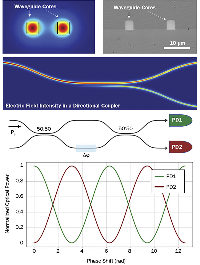
Integrated photonic platforms consist of many building blocks, such as directional couplers, that can be combined to create full on-chip Mach-Zehnder interferometers. Courtesy of vario-optics.
The other primary use case of photonics in sensing devices takes advantage of the evanescent field, which is present in single-mode waveguides and permits the use of interference effects.
The countless applications and possibilities of interferometric sensors are well known. It is a powerful and precise technique to measure the tiniest variations at several scales, from the roughness of optical surfaces to the detection of gravitational waves in kilometer-size interferometers. In all of these cases, the stability of the interferometric system (i.e., its isolation from parasitic environmental fluctuations) is critical.
An interferometer incorporated on an integrated photonics platform eliminates most moving parts and therefore exhibits inherent benefits. The counterpart of
the central element of any interferometer — the beamsplitter — is achieved in a rather simple manner in integrated photonics. By bringing one waveguide arm into the vicinity of a second waveguide arm, a so-called directional coupler (DC) is realized. In a DC, light can couple from one waveguide arm to the other arm, resulting in an optical signal at both outputs.
Conversely, a DC can be used to superpose light from the two arms. When the two optical signals stem from a reference and a measurement arm, for example, they create a superposed interference signal. The strength of this interference signal depends on the phase shift between the reference arm and the measurement arm, which can be induced by several measurement parameters.
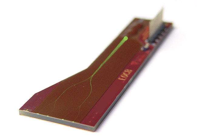
An on-chip arrangement of two such directional couplers in a row results in a highly miniaturized but complete and stable Mach-Zehnder interferometer (MZI), which is capable of detecting tiny phase shifts. With a footprint of less than 1 sq cm, this sensor can detect subnanometer optical path shifts1.
Bright future ahead
As the photonic sensing market continues to evolve, it will introduce and expand many attractive applications and possibilities for planar polymer waveguides.
Interferometry, in particular, benefits the most from integrated photonic solutions, and it holds the promise for making the leap from a laboratory-scale measurement tool to a widely employed sensor type — without needing to compromise on resolution or precision.
A good example of interferometric
sensor applications can be found in the EU Horizon 2020 PASSEPARTOUT
project. One of the project’s many goals
is to apply photothermal interferometry
to sense black carbon aerosols using a system so miniaturized that it can be carried by a drone. The overall aim is to enable real-time pollution monitoring in cities and other environments.
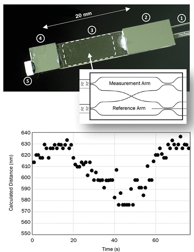
An example of an on-chip Mach-Zehnder interferometer used as a miniaturized displacement sensor. Courtesy of vario-optics.
After several years of intensive R&D, planar polymer waveguide technology has overcome one main obstacle to broader market adoption: It now accommodates a seamless design and workflow process that allows virtually anybody to access and make use of integrated photonics in electro-optomechanical systems, independently of their expertise level in optics. Key to this development was the modularization and standardization of optical components.
A variety of such EOCBs are used in the field today, and many have proved to outperform their purely electronic counterparts. As for many other integrated photonic technologies, developing efficient optical interfaces of EOCBs with other components, such as lasers and transceivers, is still an evolving field that will eventually benefit from the ongoing
efforts on standardization of such interfaces. This also applies to the materials science, where extended wavelength ranges and low-loss materials are under development.
All in all, it is a common perception that this technology will have a deep and long-lasting impact on the sensing and telecommunications markets.
Reference
1. J. Kremmel et al. (Aug. 23, 2018). Passive aligned assembly of an integrated optical displacement sensor based on a reflective Mach-Zehnder interferometer with a 3 × 3 directional coupler. Opt Eng, Vol. 57, Issue 8, p. 087103, www.doi.org/10.1117/1.oe.57.8.087103.
Meet the authors
Nikolaus Flöry, Ph.D., is business development manager at vario-optics, where he works on
integrated photonics applications based on the company's unique polymer waveguide platform. He holds a master’s degree in physics and a doctorate in optical sciences, both from ETH Zürich; email: [email protected].
Thomas Hughes is senior photonics development engineer at vario-optics, where he is responsible for the scale-up of waveguide manufacturing processes. He holds a diploma in microsystems technologies from the
University of Applied Sciences Mittweida; email: [email protected].