Liquid crystal technology and MEMS are enabling reprogrammable PICs that will be able to support multiple functions and significantly accelerate the development cycle of future photonic chips.
WIM BOGAERTS, GHENT UNIVERSITY
While electronics are perfect for performing fast calculations, photonics are ideal for moving information around. A major drawback of the latter, however, is the slow and costly development process for new photonic integrated chips, hampering their widespread use. If photonic chips could be reprogrammed for different applications, this would drastically lower development costs, shorten the time to market, and improve the sustainability of their use.
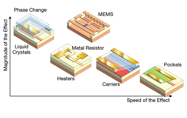
The various approaches ranked according to the speed of the phase shift effect they enable versus its relative magnitude. Different actuation mechanisms can implement phase shifting in photonic circuit platforms. The ideal phase shifters would offer low power consumption, low optical losses, a short optical length, and a small footprint. Stronger mechanisms typically require a smaller footprint or length to include a phase shift. Courtesy of Ghent University/imec.
In order to operate, reprogrammable photonic chips would require a large number of efficient electro-optic actuators to switch, split, and filter the light signals traveling through them. By introducing microelectromechanical systems (MEMS), as well as liquid-crystal-based solutions, researchers are now developing low-power building blocks for large-scale and reconfigurable photonic integrated circuits (PICs). Such versatile photonic chips promise to expedite applications in a wide variety of industries, including biosensing, medical technologies, and information processing.
A bottleneck for innovation
Over the past five decades, we have witnessed a real electronics revolution. Electronics are now powering many fundamental activities in society. Photonics technology is now ramping up to go through a similar boom. Emerging PICs are increasingly essential to powering today’s communications networks and data centers. At the same time, the complexity of these components is also rapidly growing. A single photonic chip now boasts tens or even hundreds of thousands of building blocks.
However, in contrast to the world of electronic chips, where it is possible to buy off-the-shelf chips and program them to perform a variety of functions in various applications, most PICs are application specific. The circuits defining the light paths on the chip are set during the design phase for optimal performance for a particular function and fabricated as designed. This leaves no flexibility for reprogramming and makes it almost impossible to repurpose a photonic chip for a different purpose. Instead, every new application requires a new chip design.
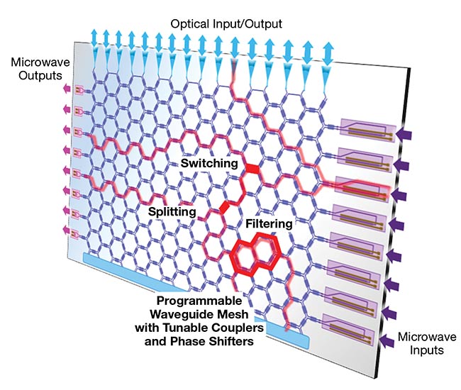
A programmable photonic circuit. The flow of light on the chip is controlled through a mesh of optical gates consisting of tunable couplers and phase shifters. By routing light between different functional building blocks and distributing it over various paths, it becomes possible to implement a variety of functions, including wavelength filters. Courtesy of Ghent University/imec.
The design, manufacturing, and test cycle of a photonic chip is slow and costly. It can easily take 12 months before the results of a chip fabrication run are known. And because the photonics ecosystem is not yet as mature as that of electronics, the fabricated chips do not always work as intended, especially in the first iterations of very complex circuits.
Consequently, it can easily take five to six years to develop an idea into an actual product, depending on the objectives and the number of chip iterations needed to succeed. This timescale poses an enormous entry barrier to innovators who want to bring photonic chip technology into new application domains. Today, PICs are primarily used in telecom and datacom settings. While there have been exciting demonstrations of PICs for sensing, spectroscopy, lidar, and quantum information processing, the number of actual commercial PIC-based products in these diverse application fields is still in the single digits.
One possible solution to break this stalemate and lower the barrier to entry is to introduce programmability into photonic circuits.
Again we can look at the example of electronics. Multipurpose programmable electronics, such as field-programmable gate arrays (FPGAs), have been a crucial enabler for innovation in consumer electronics. Photonics needs chips with a similar use model: Buy a general-purpose, off-the-shelf chip and then configure it to perform the optical functions needed. A programmable photonic chip such as this could bring down the prototyping timeline for a new photonic product from many years to a few months or even weeks. This will lead to an enormous boost in the use of photonic chips and the diversity of their applications.
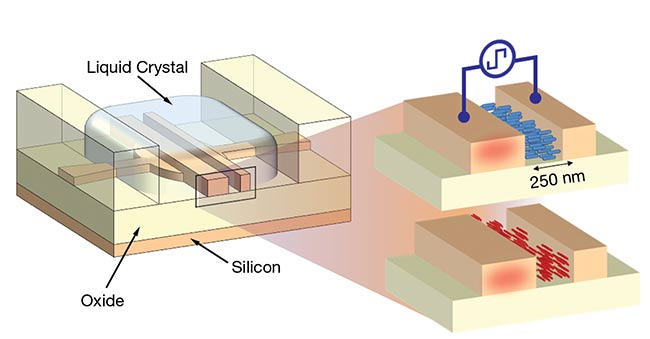
Liquid crystal actuation. A silicon rail next to the waveguide acts as an electrode to reorient the liquid crystal in the gap. This induces a phase shift for the light passing through the waveguide. The liquid crystal is locally deposited into small on-chip cavities using inkjet printing (top). To characterize the phase shifter, it is embedded in one arm of an imbalanced Mach-Zehnder interferometer (bottom). Courtesy of Ghent University/imec.
Ghent University, imec, and other organizations are pursuing collaborative projects to create such generic programmable photonic chips. Like application-specific chips, these come with their own set of new challenges.
To make the paths of light on the chip configurable, it is necessary to incorporate hundreds of thousands of optical gates that are controlled by electrically tunable phase shifters. These phase shifters can induce tiny delays in the various paths of light, which then leads to constructive or destructive interference of the optical waves and causes the optical signals to change their paths. Thus, the optical gates act as microscopic switches that couple two inputs and two outputs, with the added ability to continuously tune the splitting of light within the range of 0% to 100%, and also provide control over the optical phase. Such full control comes at a price: These basic building blocks need to perform extremely well because light has to pass through a long chain of phase shifters.
MEMS and liquid crystals
The conventional way to implement an optical gate on a photonic chip is to use microheaters. These are tiny electrical heaters positioned close to the waveguide. Heating up a waveguide changes its optical properties, inducing a phase shift. Even though these heaters are very small, they each consume many milliwatts of power, which makes scaling to very large circuits difficult.
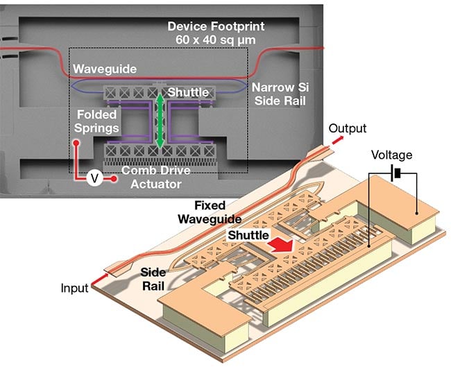
A MEMS optical phase shifter. The silicon (Si) waveguide is flanked by a thin rail of silicon. All the elements are suspended. The rail can be pulled away from the waveguide using electrostatic forces in a comb-drive actuator. When the silicon rail is farther from the waveguide, the light in the waveguide will register less silicon in the vicinity and propagate faster, thus inducing a phase shift. Courtesy of KTH Royal Institute of Technology and Ghent University/imec.
In 2018, the European Union-funded MORPHIC project kicked off with the aim to enhance programmable silicon photonic circuits with advanced waveguide MEMS. MEMS are small mechanical actuators, a few micrometers in size, that can change the distance between two waveguides. These movable waveguides can be actuated electrostatically, simply by maintaining a voltage over a capacitor. There is no static power consumption to maintain the state of the device. The optical effect of a MEMS phase shifter is very strong. Physically moving silicon structures around enables the device to create a very large change in the optical environment that the light will perceive.
The MORPHIC consortium demonstrated MEMS phase shifters and tunable waveguide couplers with lengths of only 60 µm and with power consumption levels of nanowatts. Although this was not the first time that MEMS actuators had been combined with optical waveguides, MORPHIC demonstrated the first integration of MEMS in a complete silicon photonics platform, without sacrificing the performance of other key components on the platform, such as high-speed modulators and germanium photodetectors.
This integration was less than straightforward. Where traditional silicon photonic waveguides are encapsulated within a cladding of silicon dioxide and other dielectrics, movable waveguide components must be free-standing, which means they are suspended in air or in a vacuum. The team of six European partners comprising MORPHIC resolved this issue by locally removing the supporting layer under the waveguides to make them movable, and then protecting the free-standing MEMS devices using a wafer-level hermetic sealing approach. Thus, the devices can be connected into larger circuits and electrically wired to custom-designed multichannel drivers and readout electronics using high-density interposer technology. From the wafer-scale processing all the way to the packing and programming, the researchers demonstrated that these waveguide MEMS actuators could be used as an efficient optical tuning mechanisms on a silicon photonics chip. The accomplishment required a multidisciplinary effort, involving semiconductor processing; electrical, optical, and mechanical design capabilities; and the development of multiple packaging and assembly processes, as well as software routines.
In parallel with the MEMS approach, researchers are also exploring the potential of liquid crystals for programmable photonic chips. Liquid crystal materials are birefringent, meaning they can change their refractive index by using a local electric field to reorient their liquid crystal molecules.
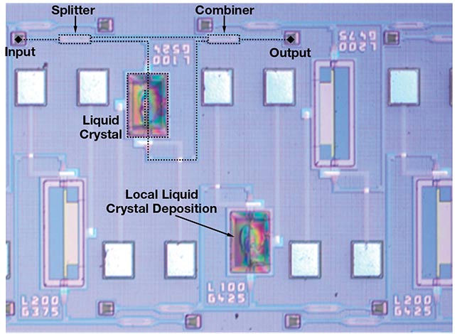
Supported by two grants from the European Research Council, researchers for the PhotonICSWARM and LIQUORICE projects successfully integrated liquid crystals on a fully functional silicon photonic chip by locally embedding waveguides in a liquid crystal cladding. The light in the waveguides registers the local rotation of the liquid crystal molecules, which can be actuated with a nearby electrode. The resultant 50-μm-long phase shifter enabled researchers to achieve a 0.8-π shift, driven by only 5 V and consuming mere microwatts of power.
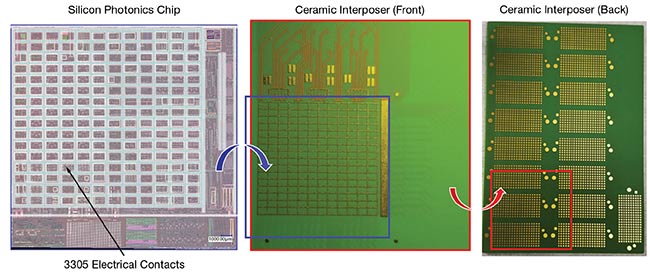
A large-scale assembly flow developed during the MORPHIC project. The silicon chip can expose up to 3305 electrical connections. These match the footprint of a large ceramic interposer that breaks out these many connections to a footprint compatible with standard printed circuit boards. Courtesy of Interposer images courtesy of Tyndall National Institute. Chip image courtesy of Ghent University/imec.
An ideal phase shifter consumes very little electrical power, imposes low optical losses, and has a footprint of minimal optical length. It also helps if the phase shifters offer a very fast, nanosecond response time and can be controlled with CMOS-compatible voltages. Meeting all of these requirements is very difficult and, to this date, there have been no demonstrations of such an ideal phase shifter. But the recent collaborative research on liquid crystal and MEMS devices offers two promising candidate technologies, and researchers are using these new phase shifters to implement larger programmable circuits.
A complete technology stack
Programmable photonics is more than a network of optical gates on a chip. Each of these actuators must be connected to driver electronics, which must be controlled through multiple layers of software, by using monitoring signals collected from on-chip photodiodes. And all of this must be brought together using a combination of optical, electrical, thermal, and mechanical packaging techniques. To realize the potential of programmable photonics, all of the elements in the technology stack must be covered.
MORPHIC wrapped up its aims in 2022, but the consortium opened a new chapter in the follow-up project PHORMIC. The team brought in additional partners to help tackle another crucial aspect of building large-scale programmable silicon photonic chips: the integration of transfer-printed optical amplifiers and light sources onto the same chip.
The amplifiers can help overcome the accumulated optical losses in the larger circuits, but they also offer the possibility of engineering programmable light sources on the chip itself.
The overarching goal of the two projects is to develop a photonic platform on which a single chip could be used to demonstrate a variety of optical functions, such as modulating or demodulating different optical communications formats, reading out optical sensor signals, or providing wavelength filters for spectroscopy applications. Combined with onboard high-speed modulators and detectors, such chip-based platforms could also implement microwave functions, which will be very valuable for next-generation 6G wireless communications networks.
The capability to use the same chip
to prototype different functions is a potential a game changer for the field
of PICs because it enables the same sort
of rapid development models that proved
so successful in the development of electronics.
The recent announcement by the Valencia, Spain-based startup iPronics
that it had commercialized the first operational photonics processor of this kind was received with great enthusiasm. The achievement shows that the photonics industry is on the right path to enabling more widespread adoption and innovation in the field of photonic integrated chips.
Meet the author
Wim Bogaerts is full professor in the Photonics Research Group affiliated with both Ghent University and imec. He coordinated the
European project MORPHIC from 2018 to 2022 and currently coordinates the PHORMIC project.
Acknowledgments
The author would like to acknowledge the researchers collaborating on the MORPHIC, PHORMIC, and LIQUORICE projects, along with the projects’ affiliated academic and industry partners.