HERZOGENRATH, Germany — Pulsar Photonics held a groundbreaking ceremony to launch construction of a corporate headquarters to be located in Aachen, Germany. The company was originally located on the premises of the Fraunhofer Institute for Laser Technology ILT (Fraunhofer ILT), also in Aachen, when it was established in 2013. The company is now based Herzogenrath, Germany.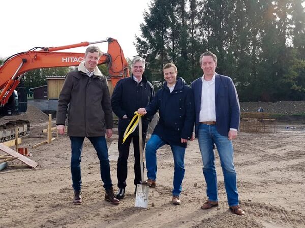
Members of Pulsar’s and Walbert-Schmitz GmbH & Co. KG’s management at the groundbreaking ceremony. Courtesy of Pulsar Photonics.
ABINGDON, England — The UK Atomic Energy Authority (UKAEA) awarded £11.6 million ($14.6 million) in support of innovative technologies for fusion energy. Nine recipient organizations were awarded a total of 10 contracts. Recipient organizations include Duality Quantum Photonics, TWI, and Oxford Sigma.
OXFORDSHIRE, England — Fusion energy scientists and engineers at the Joint European Torus (JET) developed a laser-based method to release and measure tritium trapped in fusion energy tokamaks. Fast heating the tiles in JET with a high-powered laser causes the rapid expansion and evaporation of gases retained in deposits on the tile surface. The released gases, including tritium, are then identified and measured. Though JET will be decommissioned at the end of 2023, the same laser-based techniques can be applied to future fusion machines with different in-vessel wall materials, the team said.
SANTA CLARA, Calif. — Applied Materials Inc. and CEA-Leti expanded their long-standing collaboration to focus on developing differentiated materials engineering solutions for several specialty semiconductor applications. The partners will establish a joint lab that aims to accelerate device innovations for Applied’s customers serving IoT, communications, automotive, power, and sensors markets. Technology applications in those fields include photonics and image sensors.
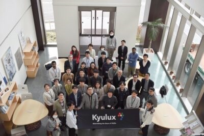
The Kyulux Fukuoka team. Courtesy of Kyulux Inc.
FUKUOKA, Japan — Kyulux Inc., an OLED emitter systems developer, raised ¥4.27 billion ($29.8 million) through a series C funding round. Kyulux will use the newly raised funds to further accelerate its product development, strengthen its IP portfolio, and progress toward its system in cooperation with affiliated chemical companies.
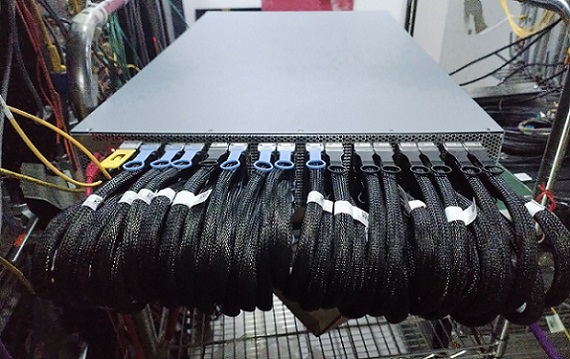
H3C’s large-scale 800GE test using the Spirent TestCenter 800G B2 Appliance. Courtesy of H3C.
BEIJING — H3C, in collaboration with Spirent Communications, completed construction of a large-scale 800GE test with a high density of up to 64 800G ports using the Spirent TestCenter 800G B2 Appliance. The goal of the test was to demonstrate aspects of H3C's 800G CPO silicon photonic switch series, H3C S9827, including overall switch capacity, full-port 100% line speed forwarding, and transmission latency.
CHANTILLY, Va. — The National Reconnaissance Office (NRO) awarded five strategic commercial enhancements (SCE) contracts to assess and leverage commercial electro-optical capabilities. Companies receiving awards under NRO’s SCE broad agency announcement framework include Airbus U.S. Space and Defense, Albedo Space, Hydrosat, Muon Space, and Turion Space. The value of these contracts was not disclosed.
STOCKHOLM — Multimodal human-machine interaction solutions developer Neonode was awarded a contract by an undisclosed commercial vehicle OEM to supply driver-monitoring system software to the OEM's global range of commercial vehicles. Neonode will provide a custom solution based on its proprietary MultiSensing platform, and will receive licensing revenues from 2025 when the first vehicles equipped with Neonode’s solution are to reach market.

The recently purchased Nomi facility. Courtesy of TOPPAN Inc.
TOKYO — TOPPAN Inc. entered into a sale and purchase agreement with OLED developer and manufacturer JOLED Inc. for the land and buildings at the JOLED Nomi Site in Nomi, Japan. TOPPAN plans to use the site for technology development and the construction of a mass production line for flip-chip ball grid arrays that meet demand for high-speed transmission and chiplet use. The company expects to launch the new line in 2027.
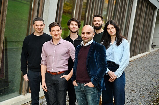
The QuantaMap team. Courtesy of QuantaMap.
LEIDEN, Netherlands — Dutch quantum technologies startup QuantaMap secured €1.4 million ($1.5 million) in early-stage funding to improve the production of quantum computer chips. The funding, which includes investment from Dutch quantum fund QDNL Participations, will help to grow the company as well as manufacture its novel microscope instrument that will allow quantum researchers and chip manufacturers to closely inspect each chip to assure and improve its quality.
LIVERMORE, Calif. — Aalyria was awarded a development contract with the European Space Agency, supported by the UK Space Agency, to help unlock 5G/6G terrestrial and nonterrestrial network capabilities. The project aims to develop a first-of-its-kind O-RAN compliant orchestration system that can stitch together disparate connectivity assets to form highly heterogeneous networks. Separately, the company partnered with LeoLabs to combine expertise and technologies to address space awareness challenges for complex communications networks that span land, sea, air, and space.