There has been a panoply of research into
the next big thing in quantum dots – those semiconducting artificial atoms
that are ubiquitous in fluorescence imaging, biological and chemical sensing, and
display applications. Quantum dots of more (or less) exotic materials and with more
(or less) interesting shapes are demonstrated on almost a weekly basis. It is the
heyday for the field. But getting less attention are the practical issues of handling
quantum dots in such a way that their functionality can be maximized and their use
more broadly commercialized.
What follows is a look at some important steps in that direction.
Dropping through the grate
Negative-refractive-index materials, superlenses and Raman scattering-based
spectroscopy are just a few applications that have come about – or that have
been improved – through research developments involving surface plasmons.
Quasiparticles analogous to photons, surface plasmons are the faint residue of electronic
oscillations that occur naturally at the interface between metal and dielectric
materials, such as silver and air, respectively. Integrate photons into the situation,
and you obtain surface plasmon polaritons, another form of energetic quasiparticle
that moves across the metal surface until reabsorbed or radiated away.
One way to improve the signal quality in a sensor is to use surface
plasmon polaritons to enhance the fluorescence signal of nearby dye particles. For
example, using a metallic surface rather than glass can improve the emission intensity
of a fluorescent dye by as much as 20 times, perhaps more. Furthermore, if the metal
surface is grated, more enhancement can be coaxed from the system because the coupling
of photons to surface plasmons is boosted.
To further increase the applicability of fluorescence enhancement
to sensor technology is to use quantum dots instead of dyes. Quantum dots have several
advantages over fluorescent dyes, including size-dependent emission spectra, wide
absorption bands, insusceptibility to photobleaching and higher quantum yields.
“In our work, we were able to take advantage of several
of the special properties of quantum dots relative to traditional fluorescent dyes,”
said Ehren Hwang of the University of Maryland, College Park. “The broadband
absorption allowed us to use a pump wavelength widely separated from the quantum
dot emission wavelength during the earlier phases of [our] experiment. We also were
able to take advantage of the intrinsic resistance of quantum dots to photobleaching,
[which] allowed us to interrogate our samples for extended periods of time –
several hours – with repeated use over the course of months.”
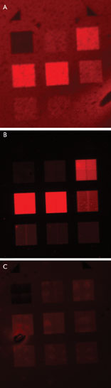
Shown, are micrographs of (A) PMMA/quantum dot composite film on gold, with an integration time of 240
s; (B) pre-spun quantum dots over PMMA on gold, 30 s; and (C) pre-spun quantum dots
over PMMA on chromium, 30 s. Courtesy of Ehren Hwang, University of Maryland, College
Park.
Hwang, his adviser, professor Christopher C. Davis, and Igor I.
Smolyaninov, now with BAE Systems in Washington, recently reported the effects of
using quantum dots instead of fluorescent dyes in these systems. They used the polymer
PMMA to create gratings over a 50-nm-thick layer of gold on glass. PMMA, the researchers
noted, is inexpensive and easy to scribe with electron beam lithography. The polymer
tends to absorb dye particles, making measurement of their positions and emissions
less than certain, but quantum dots are much bigger, don’t get absorbed into
the PMMA and, thus, are more certain when it comes to measurements.
“The physical positioning of the quantum dots was of paramount
importance,” Hwang said. “The propensity of quantum dots to remain at
the surface of the film was instrumental in enabling us to study closely the relationship
between the grating and fluorescence enhancement.” He cautioned, however,
that the size of quantum dots may be problematic for biosensing, especially if the
particles are expected to be taken up by cells. In addition, the particles also
tend to be made of cadmium or other materials that can be toxic to cells.
For some tests, the investigators directly deposited CdSe/ZnS
quantum dots onto PMMA; for others, they mixed the PMMA with the quantum dots prior
to coating the glass/gold base. The particles had an emission peak of 640 to 660
nm and quantum efficiency of 40 to 50 percent. They also tested grated and ungrated
PMMA samples and, to determine whether the surface plasmon polaritons were the sole
source of fluorescence enhancement, they made still other samples using chromium
or indium tin oxide instead of gold.
After irradiating each sample with a filtered mercury discharge
lamp, the investigators found that the gold layer clearly enhanced fluorescence
compared with the alternate materials. Interestingly, quantum dots deposited prior
to carving out the grating via electron beam lithography remained on the surface
afterward.
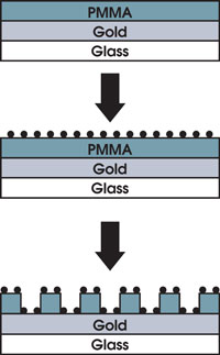
Coating a PMMA-gold-glass system with quantum dots before etching a
grating pattern into
the PMMA material makes possible novel ways to increase the sensitivity
of biosensors
based on the interactions of surface plasmon and light. Reprinted with
permission
of the American Chemical Society.
Quantum dots that were mixed in with the PMMA and that drifted
close to the gold thin-film layer were quenched, which was expected.
Overall, Hwang and his colleagues reported in the Dec. 30, 2009,
issue of NanoLetters, the thickness of the PMMA layer, the periodicity of the grating
and the grating geometry all had an effect on quantum dot-based outcomes.
According to Hwang, he and Davis now are performing experiments
to investigate the influence of the substrate material thickness on the quantum
dot enhancement effect. They also are drilling down into the nature of fluorescence
enhancement in other ways.
“If possible, we would also like to probe our substrates
using a more standard Kretschmann prism-coupling setup and to study the dependence
of the system on azimuthal rotation of the gratings relative to an off-axis illumination
source – that is, spinning the gratings around the Z-axis,” Hwang said.
Additionally, “we are interested in probing our structures using a near-field
scanning optical microscope in order to examine the near-field response of the interaction.”

Laying out an array of quantum dots with photo-oxidizable bonds, then breaking those bonds selectively
with a scanning laser, enables changes in either emission intensity (top) or wavelength
(bottom). Courtesy of James D. Batteas, Texas A&M University.
Taking a firm position
The quantum dot deposition method used by Hwang and his colleagues
is typical but, ultimately, random. You can get a layer of fairly uniform thickness
using spin-coating techniques, for example, but it is no way to get a finely arranged
array of particles with submicron resolution between particles.
The ability to precisely lay down individual quantum dots could
be the next step toward improved biosensors, but also to better LEDs, organic LEDs,
solar panels and other optoelectronics.
But it’s not easy, by any stretch of the imagination. First,
one must create the particles, then move them around individually to the desired
location. Doing this with optical tweezers would be direct, but besides other challenges,
would be dreadfully slow when spacing out an array of particles on a commercial
scale.
Instead, placing arrangements of quantum dots has typically been
done through photochemical means. One such method is to deposit quantum dots with
molecular tags, or ligands, that adhere the particles onto a substrate, then, with
lasers, chemicals or both, strip the bonds of select adherents, leaving only the
quantum dots required.
To researchers at Texas A&M University’s chemistry department
in College Station, however, this and other methods are too labor-intensive. To
address the issues, they developed a method, dubbed “lithosynthesis,”
that takes advantage of the photo-oxidation process.
According to James D. Batteas, associate professor of chemistry
and materials science and engineering, lithosynthesis is a process wherein CdSe
quantum dots are capped with a photo-oxidizable molecule, then spread onto a positively
charged glass, silicon or other substrate. When a laser scans the layered surface,
a portion of the caps are broken, leaving behind patterned arrays of quantum dots
that have various emission intensities and wavelengths.
Batteas and his colleagues report in the March 10, 2010, Journal
of the American Chemical Society that they used 16-mercaptohexadecanoic acid (16-MHA)
to cap 4-nm-diameter CdSe quantum dots and positively charged poly(diallyldimethylammonium
chloride) to enable the photo-oxidation effect in their experiments.
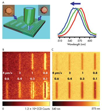
Using a 488-nm laser scanning at 0.1 to 4 μm/s, researchers
changed the emission intensity (B) and peak positions (C) of the arrayed quantum
dots. Reprinted with permission of the American Chemical Society.
Using a 488-nm argon-ion laser, they raster-scanned the landscape
of capped particles, photo-oxidizing the tandems, breaking their bonds and leaving
behind a composition of quantum dots with various intensities and wavelengths.
“This approach allows for the high spatial resolution patterning
of quantum dots in which both emission intensity and wavelength can be spatially
modified on a single layer of quantum dots,” Batteas said. “With regards
to chemical sensing, this has many advantages over carrying out these measurements
in solution.”
In particular, he noted, using quantum dots in solution often
results in their untimely aggregation and, ultimately, their precipitation. “Since
our platform is on a surface, this cannot occur.”
The group also considered ligands besides 16-MHA as caps, but
despite the prospect of lower quantum yields, found that quantum dots capped with
16-MHA exhibited a dramatic increase in luminescence after laser exposure. The researchers
also noted that the increased luminescence following photo-oxidation is reversible
by dipping the quantum dot array into a 16-MHA bath, where reconnections can occur.
Luminescence intensity changes also are affected by materials used.
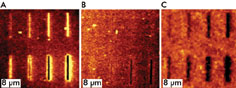
(A) shows a control sample patterned in air and soaked in CH2Cl2; (B) shows a sample
that has been immersed in 16-MHA; and (C) shows a sample that has been soaked in
porphyrin thiol solution. Reprinted with permission of the American Chemical Society.
An additional advantage to the technique is that the photo-oxidized
quantum dots become more capable of binding to newly introduced molecules than the
other, unoxidized material.
“The ability to bind new molecules to the photo-oxidized
quantum dots allows us to turn their emission on and off, allowing for data storage
capabilities,” Batteas said. “They also show the propensity to selectively
bind new molecules, allowing the modified quantum dots to be readily adapted for
chemical sensing applications.”