Rubber-like material embedded with fluorescent proteins could replace an inorganic phosphor in white hybrid LEDs.
RUBÉN D. COSTA, IMDEA MATERIALS INSTITUTE
The first advances in color displays date to the mid ’50s with the development of the cathode ray tube1, the primary display technology until liquid crystal displays (LCDs) emerged a decade ago. For a brief period, plasma technology showed promise, but ultimately it could not compete with LCDs in applications that required high contrast and low power. The superiority of LCDs stems from the use of white inorganic light-emitting diodes (LEDs) instead of fluorescent tubes as energy-saving and highly efficient backlighting components.
Nowadays, two approaches are the front runners of the LCD field (Figure 1). The first involves the development of micro-patterned films with color down-converters that partially transform the high-energy emission of the backlighting system into the desired color, enhancing both the color gamut and the brightness of the LCD displays.
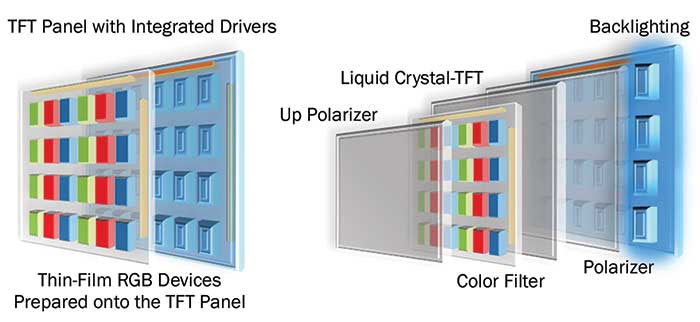
Figure 1. Schematic illustration of electroluminescence-like (left) and LCD (right) displays.
The second relates to the fabrication of displays based on the so-called electroluminescence concept — that is, the direct transformation of the externally applied current flow into light in small-sized and thin-film devices that constitute the pixels.
On the one hand, conventional LCDs require a multilayered display architecture that includes LED backlighting, light filters and polarizers, a thin-film transistor (TFT) combined with liquid crystal layers, and micro-patterned color filters, among other components. These configurations lead to an excellent lifespan in terms of color gamut and brightness and can be produced at low cost.
On the other hand, the electroluminescence displays consist of a rigorous encapsulated TFT layer used to drive a micro-sized grid of thin-film electroluminescent devices that constitute the pixels. As such, they are self-emissive, controlled by the externally applied driving current, making the use of backlighting, a polarizer and color-filter layers unnecessary2. Where there is light, there is also shadow. These days, the unbalanced lifetime of the green-, red-, and blue-emitting devices caused by the different degradation rates under electrical stress, as well as the high-cost and time-consuming production, are still major roadblocks, leading to high initial prices for electroluminescence-based displays3. However, each pixel is individually switched off/on, allowing a sharp contrast in concert with low power consumption due to the fine control of the brightness of each pixel.
Hence, although electroluminescence displays are expected to break into the market, conventional LCD displays are still the most robust technology available.
Color down-converters
Given this brief overview, there are several criteria for color down-converters required for tomorrow’s LCD displays. They include photoluminescence quantum yields (PLQYs) superior to 70 percent spanning the whole visible range and a narrow emission with a full width half maximum (fwhm) of 20 to 50 nm. They must have high thermal and photo stabilities and no change of the emission spectrum with respect to broadening and/or shifting of the maximum wavelength upon degradation. Additionally, the materials must feature a high photon flux saturation, and allow for easy and low-cost patterning of surfaces to develop micropatterned color filters.
To date, cadmium-based quantum dots (QDs) have been the leading example of down-converters (Figure 2). These materials have been optimized featuring PLQYs close to unity. This excellent luminescence feature spans the whole visible range and does not change with the temperature.
The first LEDs and displays based on QDs date back to the works of Alivisatos4 and Kim5 and co-workers. Since then, huge efforts have been conducted to further develop displays. However, the easy and low-cost fabrication of full-color QD-based LEDs has not yet been achieved. The culprit: There’s no effective upscaling protocols for patterning individual red-, green-, and blue-emitting QDs onto pixelated panels having a full control of the relationship between scale (large area panels) and resolution (the size of the pattern of less than 100 µm). This requirement has partially been met using contact printing, such as the deposition of QDs into a donor substrate that can be transferred onto an acceptor substrate using a patterned elastomer stamp (Figure 2, center)6, and photolithographic patterning, such as the preparation of a patterned substrate whose surface is modified to selectively attach a QD in a well-defined area (Figure 2, bottom)7.
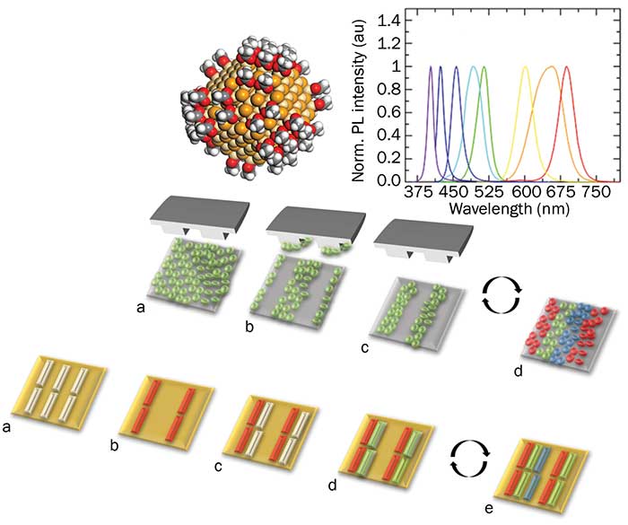
Figure 2. Upper row: Representation of CdSe QD (left) and an exemplary of the emission spectrum of several QDs spanning the whole visible range. Center row: Schematic representation of the contact-printing technique, in which the fabrication steps involve the preparation of a thin film of green-emitting QDs onto a donor substrate (a), the transferring onto an elastomeric stamp using weak interaction forces (b), the transferring onto an acceptor substrate using strong interaction forces (c) and repetition of the process with a different type of QD (d). Lower row: Schematic representation of the photolithographic technique in which the fabrication steps involve the preparation of micropatterned substrates using photolithographic technique combined with a chemical modification of the surface using, for example, self-assembly molecules to selectively attach QDs (a), functionalization of the modified surface with red-emitting QDs using spin-coating, dip-coating, etc. (b), washing of the bottom pattern and repetition of the initial photolithography-modification protocol (c), functionalization of the modified surface with green-emitting QDs using spin-coating, dip-coating, etc.(d), and repetition of the process with different types of QDs (e).
However, hurdles remain. Notably, it’s not possible to etch patterns due to the use of organic solvents in the photolithography process. The resolution of the contact-printing technique is restricted by the size of the stamp and the applied pressure. Chemical vapor deposition techniques are not possible due to the high molecular weight of the QDs.
Mass production of quantum dots
The life cycle of QD-based technologies must be considered with respect to mass production, toxicity and recycling. At the moment, there’s an ongoing debate centered on the question if the real cost for the mass production of QDs will fulfill the always-growing industry needs. There is also increased scrutiny on the limitation to a maximum allowable concentration of 100 ppm of cadmium in electrical and electronic equipment enforced by the European Union since 20038.
Nevertheless, this contrasts with the “Quantum Dot 2016 Report, Third Edition” from Touch Display Research that predicts a net worth value of the lighting market based on QDs of more than $2 billion and approximately $11 billion by 2017 and 2026, respectively9. This is surely fueled by the new trends in the QD field, such as the design of highly emissive ultralow cadmium content QDs (<100 ppm)10 and carbon-based QDs11.
Finally, it is important to point out that perovskite nanocrystals have recently started to emerge as a new type of color converter showing enhanced PLQYs across the visible range by, for example, changing the morphology from nanodots to nanoplatelets12.
Eco-friendly approach
In 2015, the use of fluorescent proteins was proposed as a new radical and eco-friendly approach13 inspired by the “green photonics” concept — the development of environmentally friendly optical systems and materials that can be applied to the current technologies to generate clean and renewable energy. Green photonics encompasses, for example, photovoltaic devices and the efficient transformation of electrical energy into light in artificial illumination systems. In this context, fluorescent proteins are the leading example. They are a sort of protein whose functionality involves the formation of visible light upon excitation of a chromophore that is embedded within the polypeptide sequence (Figure 3). They are used as biological tracers in living cells using standard fluorescence microscopy techniques.
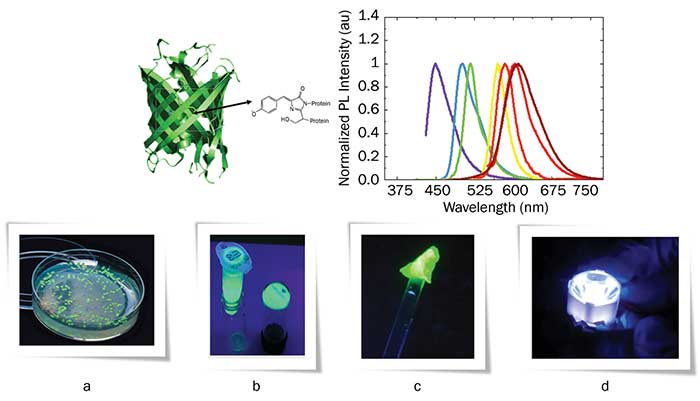
Figure 3. Upper row: Schematic representation of the green fluorescent proteins providing the chemical structure of the chromophore (left) and an exemplary of the emission spectrum of several fluorescent proteins spanning the whole visible range (right). Lower row: Pictures of a E. coli bacteria modified with green fluorescent proteins (a), an aqueous solution and hydrogel with green fluorescent proteins (b), the bio-rubber containing green fluorescent proteins (c), and a bio-WHLED under operation (d).
The main advantages of using fluorescent proteins are PLQYs superior to 70 percent spanning the whole visible range, along with the ease of color-tunability spanning the whole visible range with a narrow emission (FWHM of 30 to 50 nm). They’re also cheap to produce using E. coli bacteria, and allow easy and eco-friendly recycling using water and low-temperature procedures. The main limitations are the need for an aqueous buffer solution and the moderate stability of proteins in a solution under ambient conditions. These have strongly hampered their entrance into the lighting field since its usage for optoelectronic application was theoretically proposed in 200014.
To overcome these limitations, researchers investigated a rubber-like material in which fluorescent proteins can be embedded. The material was able to preserve the biological function of the fluorescent proteins over a much longer time span, even when they were used as down-converting materials in white hybrid LEDs (WHLEDs) under working conditions13. The key aspect is the combination of linear and branched polymers in an aqueous solution. The gel that is formed by vigorously stirring the mixture can be transformed into a rubber-like material under gentle vacuum conditions (Figure 3). These results provided the first hints that fluorescent proteins could replace the inorganic phosphor, which is used as the down-converting material in common white LEDs (WLEDs) (Figures 3 and 4). Here, commercially available UV- or blue-LEDs are coated with several layers of the eco-friendly material leading to the fabrication of bio-WHLEDs (Figure 4). In addition to fluorescent bio-components, the group was able to embed several luminescent compounds into the matrix without affecting the mechanical or luminescent properties of the matrix or emitters, respectively. They concluded that among all the down-converters applied — for example, coordination complexes, carbon QDs, polymers and laser dyes — fluorescent proteins stand out11.
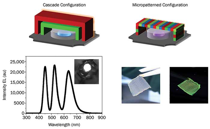
Figure 4. Upper row: Schematic representation of the bio-WHLED using a cascade-like (left) and a micropatterned-like (right) color down-converting configuration. Bottom row: Electroluminescescence spectrum of the bio-WHLED and a picture of the device working without lid (left) and a picture of the self-standing micropatterned color filter (right) under ambient and UV-excitation conditions.
A new direction: Bio-displays
Not only can the matrix be deployed in WHLEDs, but the gelatinous preliminary stage of this new matrix can be optimized itself in order to fabricate protein-based displays15. A comparison of a conventional cascade-like device and the micro-patterned bio-WHLED is displayed in Figure 4. Both have in common that instead of the LED chip, the package of the blue LED is coated with the fluorescent matrix. This architecture enables a bottom-up energy-transfer cascade mechanism, which means that the LED emits light, which is partially absorbed by the bottom layer leading to an emission at higher wavelengths. The overall emission of all layers results in the final color of the device, and it is suitable as a backlighting system.
In order to produce high-contrast and colorful displays, it is necessary to not only be able to coat different surfaces, but also to reduce the layer thickness as well as the geometry — for example, line thickness or pixel size. The defined placement of green- and red-emitting proteins on a micrometer scale was enabled using 3D printing15. Therefore, the excellent emitting properties of the proteins were combined with enhanced mechanical and rheology characteristics of the gels to allow the preparation of micropatterns with a resolution of 100 µm in a large area of 12 cm2. Finally, the luminous efficiency of the micropatterned bio-WHLED was enhanced fivefold when compared to the cascade-like devices without loss of stability. Given that the linewidth can be further reduced, micropatterned grids could be used as color filter for LCDs. In the future, the size of the bio-WHLEDs should be reduced, yielding the possibility to easily control the pixel size.
Taking into account all of the aforementioned about color down-converters for lighting and display applications, it is safe to conclude that both QDs and fluorescent proteins meet all the requirements for display applications. Although there are still some drawbacks, like the cadmium level in QDs and the low thermal stability of the fluorescent proteins, the prospect of both materials for lighting and display applications is bright.
Meet the author
Rubén D. Costa is a senior researcher at IMDEA Materials Institute, working on new electroluminescent materials, nanocarbon-based hybrids and bioinspired components for lighting, photovoltaic and sensing applications.
References
1. R.R. Thalner, Color television system, 1954, US2892019 A.
2. H.D. Kim et al. (2009). Emerging technologies for the commercialization of AMOLED TVs. Inf Display, Vol. 25, p. 18.
3. X. Dai et al. (2017). Quantum-dot light-emitting diodes for large-area displays: Towards the dawn of commercialization. Adv Mater, Vol. 29, 1607022.
4. V.L. Colvin et al. 1994, Light-emitting diodes made from cadmium selenide nanocrystals and a semiconducting polymer. Nature, Vol. 370, p. 354.
5. K.-S. Cho et al. (2009). High-performance crosslinked colloidal quantum-dot light-emitting diodes. Nat Photon, Vol. 3, p. 341.
6. T.-H. Kim et al. (2011). Full-colour quantum dot displays fabricated by transfer printing. Nat Photon, Vol. 5, p. 176.
7. J.-S. Park et al. (2016). Alternative patterning process for realization of large-area, full-color, active quantum dot display. Nano Lett, Vol. 16, p. 6946.
8. a) https://circabc.europa.eu/sd/a/187015aa-1727-48ba-b621-8273ea2b523c/ITHazardousMat.pdf; b) http://ec.europa.eu/environment/waste/rohs_eee/index_en.htm.
9. http://touchdisplayresearch.com/.
10. http://www.nanosysinc.com/press-releases-archive/2016/5/23/nanosys-introduces-hyperiontm-quantum-dots-to-unlock-displays-meeting-bt2020-color-with-high-brightness-and-power-efficiency.
11. L. Niklaus et al. (2016). Easy and versatile coating approach for long-living white hybrid light-emitting diodes. Mater Horiz, Vol. 3, p. 340.
12. L. Liu et al. (2017). Colloidal synthesis of CH3 NH3 PbBr3 nanoplatelets with polarized emission through self-organization. Angewandte Chem Int Ed, Vol. 56, p. 1780.
13. a) M.D. Weber et al. (2015). Bioinspired hybrid white light-emitting diodes. Adv Mater, Vol. 27, p. 5493. b) M.D. Weber et al. Rubber-like material for the immobilization of proteins and its use in lighting, diagnosis and biocatalysis EP-1674, 15173026.
14. Y. You et al. (2000). Fluorophores related to the green fluorescent protein and their use in optoelectronic devices. Adv Mater, Vol. 12, p. 1678.
15. L. Niklaus et al. (2017). Light-emitting diodes: Micropatterned down-converting coating for white bio-hybrid light-emitting diodes. Adv Funct Mater, Vol. 27, DOI:10.1002/adfm.201601792.