Frederic DeVriere, E2V Technologies
In recent years, low-noise CMOS imaging sensors have triggered many new opportunities and applications for the night-vision market. Although low noise is key, it is not the only parameter to consider when dealing with low-light vision. Sensitivity also is essential for the overall performance of the sensor.
Recent developments in CMOS image sensor (CIS) technology have garnered significant attention from designers of low-light devices. Although not yet able to directly compete with traditional night-vision devices (such as image intensifiers), CMOS image sensors exhibit several interesting features that make them the best solution for some parts of the market.
The technology is developing quickly and promises exciting performance in the coming years. Key to night-vision applications is noise level, which has been widely advertised as the major performance indicator – but it is not the only factor to take into consideration. Recent developments combine high-sensitivity pixel architecture with a lower-noise approach and extended wavelength response.
For many years, image intensifiers have dominated the night-vision market. They offer good performance, thanks to high amplification gain and low power consumption, but are purely analog. Digital versions involve coupling a CCD or CIS to the image intensifier.
Electron-bombarded CMOS (EB-CMOS) is now becoming a serious competitor to the image intensifier for portable digital low-light-level solutions.
Electron-multiplying CCD (EMCCD) is more focused on nonportable applications because of its need for cooling; low-light CMOS is a new solution for an application that intrinsically does not have a multiplication mechanism. This represents a drawback for photon-starved environments because it needs very low noise to be able to discriminate a relevant signal, but it makes it the perfect device for dual day and night use.
Opposite the image intensifier or EB-CMOS – which cannot operate without an amplification gain – CMOS image sensors can operate under bright illumination conditions, and features such as high-dynamic-range pixels make them even more suitable for these conditions. They also have unique advantages such as low cost, a much longer life span than other solutions, no drift of the key parameters with time, reduced pixel size (leading to lower cost integration) and high resolution.
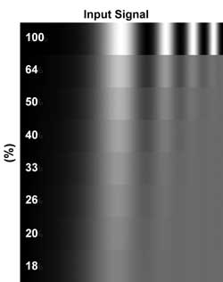
Figure 1. The effect of modulation transfer function (MTF) degradation on an image. Images courtesy of e2v Technologies.
MTF and SNR
Two parameters are driving the performances of low-light sensors: modulation transfer function (MTF) and signal-to-noise ratio (SNR).
MTF is a common way to characterize the ability of a sensor or system to provide good contrast of a scene. It is this parameter that makes the low-light CIS perform better than an image intensifier for night levels (down to night level 3), because it provides more contrasted images.
The advantage of a CIS over an EB-CMOS sensor on this parameter is also proved, but between two CMOS image sensors, the difference is not generally large.
SNR is the other key factor in the ability of a sensor to deliver a useful image. Figure 2 shows that decreasing the signal-to-noise ratio has a comparable visual effect to lowering the contrast of an image. In this figure, the eye can discriminate contrast differences down to 1/64, but noise significantly affects the perceived image.
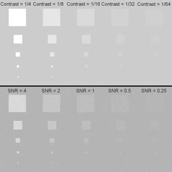
Figure 2. Decreasing the signal-to-noise ratio (SNR) has a comparable visual effect to lowering the contrast of an image.
At first glance, the sensors produce acceptable quality images with SNR = 10, and excellent images are produced with SNR = 40. Above that level, the improvement is no longer perceptible to the human eye.
For low-light environments, there are two obvious ways to increase SNR: Decrease noise, which is the approach of all low-noise sensors, and increase signal, optimizing the response of the sensor in terms of quantum efficiency, or QE – the ratio of conversion between incoming photons and measured electrons – and spectral response.
Considering the noise factor for a CMOS image sensor along with the intrinsic response of the pixel leads to the concept of noise-equivalent illuminance (NEI). It represents the minimum illuminance, or luminous flux incident on a surface, per unit area, from which it is possible to produce a usable image (SNR = 1).
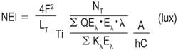
Formula 1. LT and F are, respectively, lens transmission and f number; Ti = integration time; NT = temporal noise; λ = wavelength; QEλ = spectral quantum efficiency; Kλ = the luminous efficacy; Eλ = photonic sterance; h = Planck’s constant; C = light celerity; and A = pixel area.
Using the same idea, the noise-equivalent energy (NEE) represents the energy flux incident on a surface, in lux x seconds. In this parameter, the integration time is taken into account: NEE = NEI x Ti, where Ti is the integration time. The NEI can be computed using Formula 1.
This formula shows that the weight of the QE is the same as the noise. Increasing the response of a sensor has the same effect as reducing the noise. To produce the best possible image, the sensor must be not only very low noise, but also very sensitive.
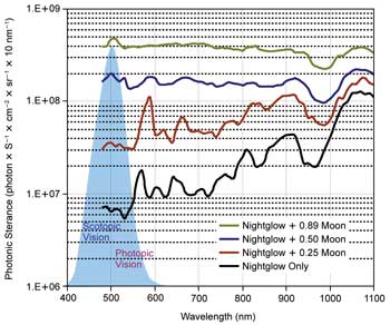
Figure 3. The illuminance of the atmosphere is more important in the near-IR region of the spectrum than in the visible. Significantly, this illuminance is less subject to atmospheric absorption than in the visible spectrum.
Practical implementation
The Ruby family of sensors from e2v (EV76C660 and EV76C661) takes the approach of improving QE and response. The overall QE of the sensors is nearly at optimum levels, and the usable wavelength extends into the near-infrared region.
Thus, the sensor can take advantage of nightglow: Under natural conditions, the illuminance of the atmosphere is more important in the NIR region of the spectrum than in the visible. Importantly, this illuminance is less subject to atmospheric absorption than in the visible spectrum (Figure 3).
Figure 4 shows that these sensors are fully optimized for spectral response to take advantage of this nightglow; therefore, they can capture much more light than traditional CMOS image sensors in outdoor environments. Investigations comparing the response curve of these sensors with that of competitors are under way.
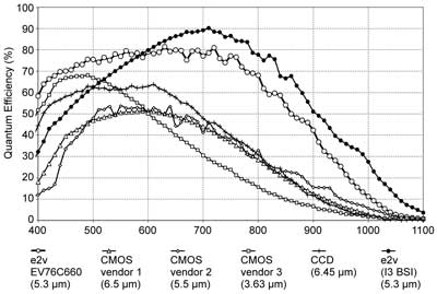
Figure 4. Ruby sensors from e2v are fully optimized for spectral response to take advantage of this nightglow. They can capture much more light than traditional CMOS image sensors in outdoor environments. A back-side illumination prototype also is represented on the curve.
The QE of the front-side illumination version is already very good, so quantum efficiency going to back-side illumination does not gain as much as it does with much smaller pixels.
For this type of sensor, the real interest of the back-side illumination lies elsewhere:
• It enables the development of specific antireflection coatings, so that the response of the sensor can be optimized on a specific part of the spectrum. In the case above, the result is shown with a near-IR-optimized coating, but it also could be applied to enhance the UV response.
• Front-side illumination requires that microlenses have good QE. They are shown to work well unless they are used with high-aperture optics, where the chief ray angle can be very high.
This sensor represents an innovative approach for night-vision and outdoor cameras. It is globally optimized to take advantage of the widest part of the light spectrum, with a silicon-based imaging device. The results are encouraging because the device can produce usable images down to night-level 3 at 25 fps, with a global readout noise of less than 6 e—.
This new type of sensor also has applications in machine-vision cameras, bar-code scanners and intelligent traffic systems.
Meet the author
Frederic Devriere is marketing manager for aerospace and defense imaging at e2v in Grenoble, France; email: [email protected].