Researchers from Helmholtz-Zentrum Dresden-Rossendorf (HZDR) have developed a low-cost broadband photodetector that uses a metal-organic framework (MOF). As it does not contain any cost-intensive raw materials, it can be produced inexpensively in bulk.
MOFs have become a coveted material system over the past 20 years for their utility in medicine due to their highly porous nature, which allows use for catalysis or to slowly release drugs in the human body.
“The metal-organic framework compound developed at TU Dresden comprises an organic material integrated with iron ions,” said Dr. Artur Erbe, head of the Transport in Nanostructures group at HZDR’s Institute of Ion Beam Physics and Materials Research. “The special thing about it is that the framework forms superimposed layers with semiconducting properties, which makes it potentially interesting for optoelectronic applications.”
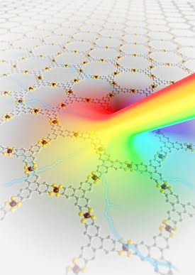
Physicists of HZDR and TU Dresden have developed a photodetector that is completely based on layers of metal-organic frameworks. Since this compound can detect and transform a broad range of light wavelengths into electrical signals, it could become a novel detector material. Courtesy of HZDR/Juniks.
To pursue the use of the MOF as a photodector, physics Ph.D. student Himani Arora investigated the semiconductor’s electronic properties, exploring the extent that the light sensitivity was dependent on temperature and wavelength. She found that between 400 and 1575 nm, the semiconductor could detect a broad range of light wavelengths. The spectrum of radiation thus goes from ultraviolet to near infrared.
“This is the first time we have proved such a broadband photodetection for a photodetector completely based on MOF layers,” Arora said. “These are ideal properties for using the material as an active element in optoelectronic components.”
The spectrum of wavelengths a semiconducting material can cover and transform into electrical signals essentially depends on the bandgap, the energetic distance between the valence band and the conduction band of a solid-state material. In typical semiconductors, the valence band is completely full, so the electrons cannot move around. The conduction band on the other hand is largely empty so the electrons can move around freely and influence the current flow. While the bandgap in insulators is so big that the electrons cannot jump from the valence band to the conduction band, metal conductors have no such gaps. A semiconductor’s bandgap is just big enough to raise the electrons to the higher energy level of the conduction band by using the lightwaves. The smaller the bandgap, the lesser the energy required to excite an electron.
“As the bandgap in the material we explored is very small, only very little light energy is required to induce the electricity,” Arora said. “This is the reason for the large range of the detectable spectrum.”
By cooling the detector to lower temperatures, the performance can be improved even further, as the thermal excitation of the electrons is suppressed. Other improvements include optimizing the component configuration, producing more reliable contacts and developing the material further.
“The next step is to scale the layer thickness,” Erbe said. “In the study, 1.7-micrometer MOF films were used to build the photodetector. To integrate them into components, they need to be significantly thinner.”
If possible, the aim is to reduce the superimposed layers to 70 nm, that is, 25 times smaller than their size. Down to this layer thickness the material should exhibit comparable properties. If the researchers can prove that the functionality remains the same in these significantly thinner layers, they can then embark on developing it to the production stage.
The research was published in Advanced Materials (www.doi.org/10.1002/adma.201907063).