Researchers from the Helmholtz-Zentrum Dresden-Rossendorf (HZDR), TU Dresden, and Leibniz-Institut für Kristallzüchtung (IKZ) have demonstrated the controlled creation of single-photon emitters in silicon at the nanoscale. According to the researchers, the technology, which is compatible with current CMOS fabrication methods, represents a promising candidate for photonic quantum technologies, with a fabrication pathway that is compatible with very large-scale integration.
Previous quantum photonics experiments required the use of “bulk optics.” These space-consuming elements would be distributed across the optical table and could occupy vast amounts of laboratory space. Now, photonic chips are changing this landscape, including for quantum photonics. Monolithic integration of single-photon sources, in a controllable way, would give a resource-efficient route to implement millions of photonic qubits in PICs. To run quantum computation protocols, these photons must be indistinguishable. With this, industrial-scale photonic quantum processor production would become feasible.
However, the currently established fabrication method stands in the way of the compatibility of this promising concept with current semiconductor technology.
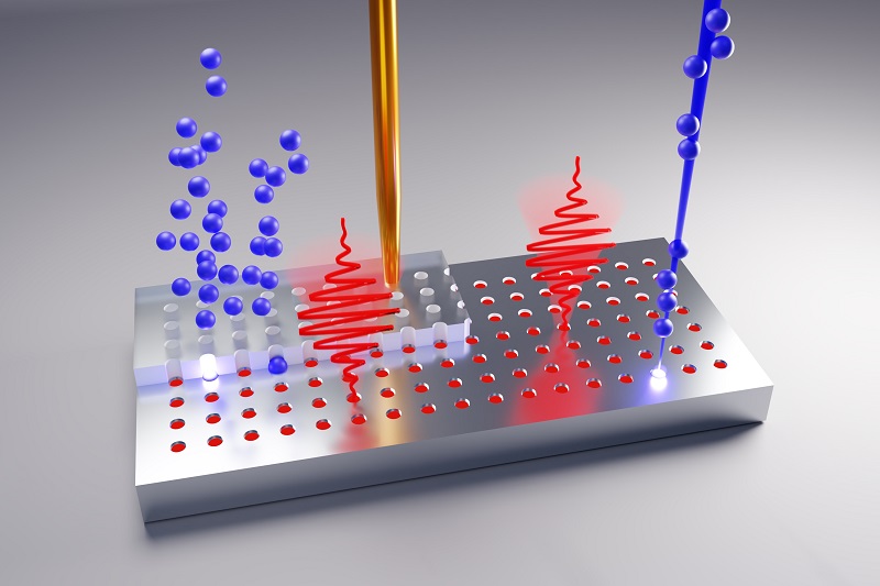
Controlled generation of single-photon emitters in silicon (red) by broad-beam implantation of ions (blue) through a lithographically defined mask (left) and by a scanned focused ion beam (right). Symbolically shown is the emission of two single photons at locations defined for this purpose by the process. In the background, an electron beam creates holes in the lithographic mask made of acrylate. Courtesy of M. Hollenbach, B. Schröder/HZDR.
In a first attempt, which was detailed in work published about two years ago, the researchers generated single photons on a silicon wafer, but only in a random, nonscalable way.
“Now, we show how focused ion beams from liquid metal alloy ion sources are used to place single-photon emitters at desired positions on the wafer while obtaining a high creation yield and high spectral quality,” said Nico Klingner, a physicist at HZDR.
Furthermore, the researchers subjected the same single-photon emitters to a rigorous material testing program. After several cooling-down and warming-up cycles, they did not observe any degradation of their optical properties. These findings meet the preconditions required for mass production.
To translate this achievement into a widespread technology and allow for wafer-scale engineering of individual photon emitters on the atomic scale compatible with established foundry manufacturing, the researchers attained broad-beam implantation in a commercial implanter through a lithographically defined mask. According to Ciarán Fowley, cleanroom group leader and head of nanofabrication and analysis at HZDR, the development allowed the researchers to use both the silicon-processing cleanroom as well as electron beam lithography machines.
Using both methods, the researchers reported that they can create dozens of telecom single-photon emitters at predefined locations with a spatial accuracy of about 50 nm. The units emit in the O-band and exhibit stable operation over days under continuous-wave excitation.
These single-photon emitters are now technologically ready for production in semiconductor fabs and incorporation into the existing telecommunication infrastructure, the researchers said.
The research was published in Nature Communications (www.doi.org/10.1038/s41467-022-35051-5).