Photonics HandbookTech Pulse
Rice Researchers Investigate 2D Materials for Maximum Optical Response
Rice University scientists have used qualitative analytical modeling and first-principles calculations to determine the theoretical limit of the maximum optical response in 55 different 2D materials. The study suggests several 2D materials that could be used in ultrathin reflectors and absorbers for optoelectronic applications.
The researchers modeled properties including transmittance (T), absorbance (A), and reflectance (R) — collectively dubbed TAR — and conducted a computational survey to seek out the materials with the best A and R in various frequency ranges, from MIR to deep-UV.
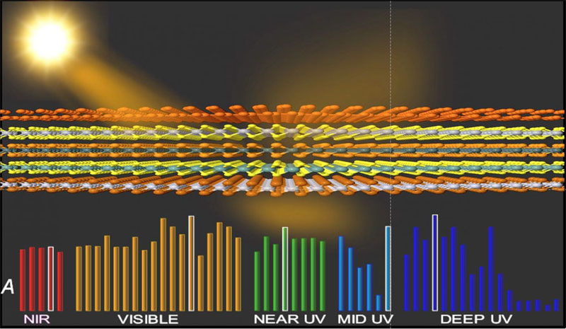
Rice University researchers modeled 2D materials to quantify how they react to light. They calculated how the atom-thick materials in single or stacked layers would transmit, absorb, and reflect light. The graphs above measure the maximum absorbance of several of the 55 materials tested. Courtesy of Yakobson Research Group/Rice University.
2D materials are used to refine the modulation and manipulation of light in optoelectronics devices. “Generally, the common wisdom is that 2D materials are so thin that they should appear to be essentially transparent, with negligible reflection and absorption,” professor Boris Yakobson said. “Surprisingly, we found that each material has an expressive optical signature, with a large portion of light of a particular color (wavelength) being absorbed or reflected.”
The researchers modeled 2D stacks as well as single layers and verified that stacks of graphene and borophene were highly reflective of MIR light. They also discovered that a material made of more than 100 single-atom layers of boron — which would still be only about 40 nm thick — could reflect more than 99 percent of light from the IR to the UV, outperforming doped graphene and bulk silver.
“Stacks can broaden the spectral range or bring about new functionality, like polarizers,” researcher Alex Kutana said. “We can think about using stacked heterostructure patterns to store information or even for cryptography.”
Knowing how sensitive a material is to a particular wavelength of light, from IR to visible to UV, could help researchers manipulate 2D materials to design devices like sensors or light-driven circuits at increasingly smaller scales. At the nanoscale, light can interact with materials in unusual ways, prompting electron-photon interactions or triggering plasmons that absorb light at one frequency and emit it at another.
“The important thing now that we understand the protocol is that we can use it to analyze any 2D material,” researcher Sunny Gupta said. “This is a big computational effort, but now it’s possible to evaluate any material at a deeper quantitative level.”
The researchers see photodetectors, modulating devices, and polarizing filters as possible applications for 2D materials with directionally dependent optical properties. For example, multilayer 2D coatings could be used to provide protection from radiation or light from lasers. In the case of laser light, heterostructured films might be needed, said researcher Sharmila Shirodkar. “Greater intensities of light could produce nonlinear effects, and accounting for those will certainly require further research,” he said.
There’s a side benefit that fits with Yakobson’s artistic sensibility as well. “Now that we know the optical properties of all these materials — the colors they reflect and transmit when hit with light — we can think about making Tiffany-style stained-glass windows on the nanoscale,” he said.
The research was published in ACS Nano (doi:10.1021/acsnano.8b03754).
Published: September 2018