
Rockley Photonics Completes Financial Restructure: Week in Brief: 06/09/23
GENEVA, June 9, 2023 — Semiconductor technology companies STMicroelectronics and Sanan Optoelectronics signed an agreement to create a 200-mm silicon carbide device manufacturing joint venture in Chongqing, China. The fab is expected to begin production toward the end of 2025 and full buildout is expected in 2028. The total cost of the buildout is expected to be approximately $3.2 billion, including capital expenditures of about $2.4 billion over then next five years, which will be financed by contributions from the two companies, local government support, and loans to the joint venture.
OXFORD, England — Rockley Photonics completed a comprehensive financial restructure and emerged from Chapter 11 after filing for bankruptcy protection earlier this year. Rockley’s material customer relationships remain in place, the company said, and it remains on schedule with all programs including its development of remote patient-monitoring technology. The company said that it also secured $35 million of additional funding from its stakeholders.
BILLERICA, Mass. — Materials technology and process solutions company Entegris broke ground on a manufacturing center of excellence in Colorado Springs, Colo. The campus will be built in phases with initial commercial operation targeted for early 2025. The 100,000-sq-ft facility will be built in the initial phase and will support production for Entegris’ Microcontamination Control (MC) and Advanced Materials Handling (AMH) divisions. Entegris expects to invest approximately $600 million in phases over several years in the facility.
TUCSON, Ariz. — Directed energy company Applied Energetics, a developer of ultrashort-pulse laser solutions, was awarded a $1.1 million Phase II Small Business Technology Transfer contract by the U.S. Army. The contract will continue the company’s research, development, and testing of an ultra-broadband infrared source capable of disrupting optical infrared sensors within the engagement time window at tactically relevant ranges.
CORK, Ireland — Tyndall National Institute partnered with the University of Galway on a €1.2 million ($1.3 million) project, Pulsed Laser Annealing of 2D Semiconductors for Nanoelectronics. The project will research the area of advanced and smart manufacturing, and will aim to substantially increase the scalability, functionality, performance, and energy efficiency of electronic devices while keeping full compatibility with existing mass production technologies.
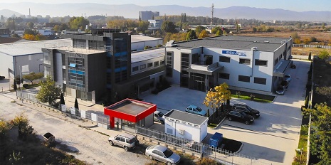
MOEMS developer ESCATEC will open a site in Plovdiv, Bulgaria, to support its production commitments in Europe. Courtesy of ESCATEC.
PENANG, Malaysia — ESCATEC, a developer of micro-opto-electromechanical systems (MOEMS), is establishing a new production facility in Bulgaria. The 4000-sq-m facility in Bulgaria is already operational with the necessary equipment, processes, and workforce to vertically integrate plastic molding and electronics assembly. The site supports ESCATEC’s production commitments in Europe.
CAPE CANAVERAL, Fla. — Sidus Space, a space and defense as-a-service satellite company, will launch hyperspectral and multispectral imaging and edge AI in its LizzeSat satellite on SpaceX Transporter missions beginning in 2024. LizzieSat’s hyperspectral and multispectral imaging capability will be provided by the Owl 1280 and Hawk 1920 HD cameras made by Raptor Photonics. Sidus is building its space-based infrastructure of multimission satellites with hyperspectral, multispectral, and other sensors to provide monitoring services and solutions to multiple sectors and industries.
/Buyers_Guide/STMicroelectronics/c32873
/Buyers_Guide/Rockley_Photonics_Ltd/c31471
/Buyers_Guide/Entegris_Inc/c4425
/Buyers_Guide/Applied_Energetics_Inc/c18272
/Buyers_Guide/ESCATEC_Switzerland_AG/c25159