Silicon on insulator — today a standard in the electronics industry — is fast becoming the platform of choice for a photonics-based technological era.
CÉLINE CAILLER, ALAIN DELPY, AND CORRADO SCIANCALEPORE, SOITEC
Silicon has been the mainstay of micro-nanoelectronics since the late 1950s, being widely adopted for electronic devices and complementary metal oxide semiconductor (CMOS) technologies. In the early years of the semiconductor industry, germanium was the favored material for electronic applications due to its higher carrier mobility; however, innovations at Bell Labs in surface passivation by thermal oxidation processing enabled a breakthrough in silicon semiconductor technology in the second half of the 1950s. Thermally grown silicon dioxide layers significantly reduce the concentration of electronic states at the silicon surface to electrically stabilize such interfaces. This capability has helped fuel broad adoption of silicon as the main vector of Moore’s law in CMOS technology, driving its democratization to mass-market applications.

Courtesy of SOITEC.
Notwithstanding its excellent properties for CMOS technologies, however, silicon was never meant to remain a purely electronic material.
In the early 2000s, an optical age
of silicon began to unfold1. The material’s broad transparency that spanned the short- and mid-wavelength infrared enabled silicon-based optics to blossom into a wide variety of photonics technologies that targeted applications in data communications, sensing, and advanced computing.
In optical communications, for example, the progressive adoption of power-efficient, high-speed, silicon photonic links has helped to address the growing demand for data transmission bandwidth and increase computing capabilities. The intrinsic capability of light to transmit signals with low latency and power dissipation, at ultrahigh data rates, can be scaled from backbone infrastructures to rack-level optical links, down to chip-to-chip photonic interconnects. However, silicon could not meet the necessary requirements of these integrated optics applications without the additional innovation of silicon-on-insulator (SOI) technology.
SOI photonics
The SOI material platform offers considerable advantages by leveraging the highly mature ecosystem of CMOS technology, as well as comparatively newer processing technologies that enable the transfer of very thin layers of material from one substrate to another. The so-called Smart Cut process, collaboratively developed by CEA-Leti and SOITEC, underlies the development of engineered wafers by stacking extremely thin (from 10 nm up to a few hundred nanometers) and perfectly uniform crystalline layers of semiconductors that could not be achieved using classic microelectronic technologies.
Based on this process, SOI technology can now replace traditional copper lines in data interconnects with submicrometer-wide silicon waveguides that send, receive, and process information using optical frequencies.
Furthermore, thanks to its inherent CMOS-compatibility, the SOI platform provides a cost-effective approach for optical chip design and high-volume manufacture that features scalable bandwidth, footprint, and functionality.
Beyond optical transceivers for the data center interconnect (DCI) market — which is today the technology’s most mature segment — SOI photonics is also enabling applications in novel computing architectures, Internet of Things (IoT) components, biosensors, and lidar systems. It will soon support advancements in quantum technologies.
By leveraging mature semiconductor manufacturing methods, engineered wafers that incorporate SOI technology offer a powerful approach toward broader adoption of integrated optics.
Basically, high-quality single-crystalline silicon layers ranging in thickness from a few nanometers to several microns can be transferred onto a buried oxide (BOX) layer that is wet-grown onto a silicon handle substrate. In photonics applications, the BOX layer ensures high optical isolation, passivation of surface states, and extremely low defect density, while the handle substrate provides mechanical stability. Notably, such manufacturing methods can scale SOI technology to 200- and 300-mm wafer formats to combine high-throughput manufacturing capability with standard CMOS processing, enabling the integration of digital and photonic functions (Figures 1 and 2).
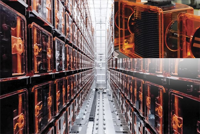
Figure 1. A production line of 300-mm silicon-on-insulator (SOI) wafers at SOITEC in Bernin, France. Courtesy of SOITEC.
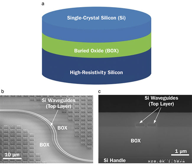
Figure 2. A schematic view of a photonic SOI substrate (a). A tilted scanning electron microscopy view of a silicon waveguide fully etched into the top silicon layer (b). A cross-sectional SEM image of a twin-waveguide directional coupler etched into the top silicon layer (c). Courtesy of CEA-Leti.
Additionally, the Smart Cut process allows further integration of advanced materials on silicon and other substrates. These materials include germanium on insulator, group III-V compounds such as gallium arsenide and indium phosphide, and piezoelectric materials such as lithium tantalate or lithium niobate. All pave the way to optical systems that offer high-performance emission, modulation, or detection of light along with industrial scalability.
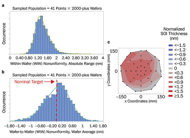
Figure 3. Within-wafer (a) and wafer-to-wafer (b) statistics of thickness nonuniformity in the top silicon layer on 300-mm photonic SOI wafers. A sampled population of over 2000 wafers is reported, while the data has been measured via 41-point wafer-scale ellipsometry (c). Specifically, within-wafer nonuniformity (a) reports the absolute range when considering all measured points among the whole wafer population, while wafer-to-wafer nonuniformity (b) refers to the 41-point average thickness deviation of each wafer with respect to the nominal target (red dashed line). Courtesy of SOITEC.
SOI technology is still evolving today to offer new capabilities for silicon photonics. For example, control over the thickness of silicon layers (Figure 3) has continuously improved to allow greater uniformity within a few nanometers and provide ideal optical behavior at both the device and circuitry levels. Similarly, silicon layer surface roughness (Figure 4) can be controlled at the atomic scale to minimize unwanted scattering and to stabilize waveguide index and the phase of optical signals. These properties are essential for low-loss and high-coherence applications, such as quantum silicon photonics or solid-state chip-based lidar.
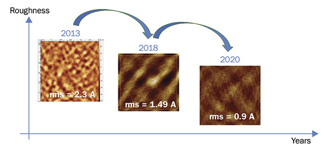
Figure 4. Top-layer silicon surface roughness measured with 30- × 30-µm atomic force microscopy scans, showing SOI evolution over the last few years. Today, processing technology can deliver 300-mm photonic SOI wafers with angstrom-level hill-to-valley surface roughness, providing cutting-edge material quality to integrated optics applications. Courtesy of SOITEC.
Moreover, as Figure 3 shows, local nonuniformity should be managed at both within-wafer and wafer-to-wafer levels to increase fabrication yields and drive down production costs for silicon photonic chips. This is particularly important when scaling up for high-volume manufacturing.
The adoption of optics-based input/outputs will ultimately
provide server architectures with greater system
flexibility, scalable speeds, and cost-effective operations
that only CMOS-compatible SOI photonics can deliver.
With regard to manufacturability, the geometrical aspects associated with SOI wafers are also of critical importance. Managing the warp and bow of SOI substrates is essential in foundry equipment, including etching and lithography tool sets used for defining submicrometric silicon features.
Maintaining all of these SOI specifications is instrumental to controlling process window stability and optimizing fabrication yields for silicon photonics.
Reaching the core
With the advent of 5G networks, the steady growth of data traffic in today’s telecommunications infrastructures is driving increases in both transmission rates and computing capabilities2. Such a burst in data is challenging the ability of short-reach copper-based interconnects in data centers and server architectures to offer enough bandwidth at reasonable power dissipation. Optics-based telecommunications has the potential to solve this challenge, if photonic functionalities can be integrated on electronic chips and cards to help trigger the onset of a photonics-based computational era. Silicon photonic integrated circuits would pave the way toward a new framework for optoelectronics that offers a significant integration potential with cost-effective CMOS electronics. Moreover, the strong refractive index contrast between silicon and silicon dioxide (n ~ 2) offered by the SOI material platform enables flexible implementation of multiple optical functions within small footprints. The index contrast offers the potential to integrate devices such as waveguides and resonators, semiconductor lasers and amplifiers, chip-to-fiber couplers, high-speed modulators, and silicon germanium photodetectors, as well as filters and wavelength
(de)multiplexers.
Silicon photonics pluggable transceivers have contributed to the exponential growth of cloud services. The introduction of co-packaged on-board optics further promises to usher in a new wave of disruptive advancements in artificial intelligence at the network edge and in high-performance computing. This more recent development is on track to unfold this year, according to industrial players in datacom. In fact, inherent limitations in the copper-based serializer/deserializer (SerDes) technology used for data input/outputs (I/Os) in today’s server switching cores will fuel further interest in shifting optics down to the core of electronics. At a later stage, SOI photonics could contribute to the paradigm shift in data center architecture by introducing “fiber-to-the-processor” optical chiplets (opto-chiplets). Such novel rack-scale computing architectures would make data centers more flexible, allowing them to pool resources by using fast, low-latency optical I/Os between CPUs, ASICs (application-specific integrated circuits), storage, and memory blocks. In this sense, the adoption of optics-based I/Os will ultimately provide server architectures with greater system flexibility, scalable speeds, and cost-effective operations that only CMOS-compatible SOI photonics can deliver.
According to Yole Développement, the silicon photonics market is expected to reach $4 billion in 2025. Market research firm LightCounting estimates that 400GbE transceiver revenues in the datacom market, which includes DCI transceivers, will reach $12 million within the same time span.
The progressive adoption of opto-chiplets based on silicon photonics would reinforce these trends. It is therefore not surprising that silicon photonics is increasingly perceived as a strategic asset by a growing number of equipment manufacturers and cloud service end users, including tier-one players in data communications technology. Electronics chipmakers and major foundries worldwide are extending their positions to master the design and processing of photonic components using SOI-based wafer technology on both 200- and 300-mm wafers. Additionally, to support high-data-rate optical communications and advanced computing applications, the industry is collaborating on a set of specifications for new high-capacity communications standards to ensure a unified supply chain.
Sensing and advanced computing
Beyond the datacom market, the benefits of silicon photonics are helping to address new applications within the sensing and advanced computing sectors.
Chip-scale optical sensing can offer considerable advantages over bulky conventional solutions that rely on the expensive heterogeneous assembly of multiple, discrete components. The rising demand for advanced driver assistance systems and autonomous vehicles in the automotive, transportation, and industrial robotics markets is increasing demand for inexpensive, industrially scalable optics-based solutions. Such solutions combine the capability of photons to sense and quantify information about the physical world without suffering from electromagnetic interference or other detrimental effects typically associated with radio-frequency waves. Moreover, SOI photonics offers a more advantageous sensing platform that monolithically integrates hundreds of devices onto the same chip. Chip-scale solid-state lidar technology is another significant driver for SOI photonics development.
With regard to biosensing technology, advanced semiconductor microfabrication allows for the miniaturization of lab-on-a-chip components. Such developments have allowed silicon-based optical biosensors to make significant progress in point-of-care diagnostics. SOI photonics will contribute to these trends by supporting development of evanescent field biosensing technologies that incorporate interferometers, Bragg gratings, micro-cavities, and photonic crystal-based waveguide sensors.
SOI-driven photonic platforms can also support a broad panel of sensing mechanisms for analyte inspection based on real biomarkers for label-free detection. Lab-on-a-chip photonic sensing platforms further enable monolithic integration of optical devices, microfluidic delivery channels, and readout equipment. These applications for system-level chip packaging collectively illustrate the potential to industrialize low-cost, high-yield, portable biosensing platforms by leveraging CMOS processes.
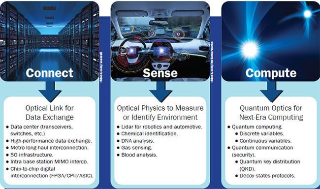
The Silicon Photonics Applications Space. Courtesy of SOITEC.
Lastly, when it comes to advanced computing, integrated photonics is increasingly seen as an attractive platform for quantum information processing. In quantum cryptography, for example, photons can act as vectors of information due to their long coherence times at room temperature and their ability to be transmitted over existing optical fiber infrastructures. Quantum correlation of photon pairs via time-energy entanglement has already been demonstrated on the SOI platform via silicon ring resonators. Combined with the large effective nonlinearities achievable in SOI waveguides, this would allow the reduction of an emitter’s footprint by orders of magnitude over non-photonics-based sources3.
Future perspectives
Silicon is positioned to become a common bridge between the fast-growing opportunities for photonics and the industrial maturity of electronics. The SOI material platform offers considerable advantages in this context because it can leverage the maturity of CMOS technology and its ecosystem.
In addition to pluggable transceivers, SOI-based photonics exhibits significant potential to enable or enhance a variety of industrial applications, including chip-scale optical interconnects for novel computing architectures, as well as
IoT, biosensor, lidar, and quantum technologies.
To enable and support the industrialization and adoption of silicon photonics, SOI technology will need to address key challenges, such as ensuring cutting-edge material quality and supporting high-
volume manufacturability. The decades-long optical age of silicon has shown that material technology and industrial success cannot run separately. This is why continued advancements in SOI technology are critical to maintaining market penetration for silicon photonics, triggering future waves of photonics-based innovation and technologies.
Meet the authors
Céline Cailler received a Master of Science in semiconductor materials engineering from Institut National des Sciences Appliquées in Lyon, France, in 2002; she joined SOITEC shortly after. Since 2011, Cailler has led SOITEC’s silicon photonic substrates, roadmaps, and customer programs as a product manager within SOITEC’s Specialty-SOI Business Unit; email: [email protected].
Alain Delpy’s microelectronics experience ranges from design to marketing in the areas of industrial and consumer applications. He joined STMicroelectronics in 1997, focusing first on communications devices and imaging, and later on x-ray spectrometry. In 2018, Delpy joined SOITEC as business development manager for imagers, silicon photonics, and MEMS; email: [email protected].
Corrado Sciancalepore, Ph.D., is a photonics materials expert within the Specialty-SOI Business Unit at SOITEC. He was previously
a permanent researcher in photonics and
optoelectronics at CEA-Leti. He is the author of more than 80 journal articles and international conference proceedings on cutting-
edge silicon photonic circuits, III-V optoelectronics, and VCSEL photonics; email: [email protected].
References
1. G. Reed (2004). The optical age of silicon. Nature, Vol. 427, pp. 595-596, www.doi.org/10.1038/427595b.
2. M. Asghari and A.V. Krishnamoorthy (2011). Silicon photonics — energy-efficient communication. Nat Phot, Vol. 5, pp. 268-270.
3. D. Grassani et al. (2015). Micrometer-scale integrated silicon source of time-energy entangled photons. Optica, Vol. 2, Issue 2, pp. 88-94.