By Laura S. Marshall, Managing Editor, Photonics Spectra
ORLANDO, Fla., April 9, 2010 — "We are in a period of significant change and uncertainty," said Zachary J. Lemnios during his symposium-wide plenary lecture Tuesday morning at the SPIE Defense, Security & Sensing conference and trade show.
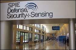
The SPIE Defense, Security & Sensing 2010 conference and trade show was held at the Marriott World Conference Center in Orlando April 5 to 9. (Photonics Media photos by Laura Marshall)
To that end, he described the new DDR&E imperatives: to accelerate the delivery of technological capabilities to win the current fight; to prepare for an uncertain future; to reduce the cost, acquisition time and risk of the major acquisition programs; and to develop world-class science, technology, engineering and mathematics (STEM) capabilities for the DoD.
World-class STEM endeavors relating to the defense and security industry were the focus of the annual DS&S conference and trade show, which brings together more than 6000 attendees for talks and events on wide-ranging topics. The accompanying exhibition drew more than 500 companies, and while many said the exhibition was slower this year than last, they also said that it was likely due to the quality of the technical talks offered.
Technical talks
The talks this year spanned a huge range of technologies and applications, from lasers to optics to imaging, from threat detection to surveillance to data display.
The word "sensing" does make up one third of the conference's name, and sensing technologies were heavily represented this week.
Raman instruments based on dispersive technology with excitation wavelengths beyond 785 nm or 810 nm have been all but nonexistent, but William Yang of BaySpec Inc. discussed recent advances in high-volume optical telecom device manufacturing that will help analysts bring the lab right to the sample with longer-wavelength excitation Raman spectroscopic analyzers.
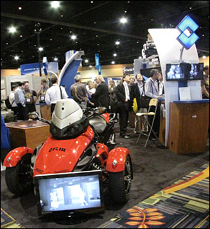
A number of companies, including Flir, had elaborate displays at DS&S 2010.
Taiichi Otsuji of Tohoku University in Japan discussed recent advances in emission and detection of terahertz radiation using 2-D plasmons in semiconductor heterostructures as well as possible applications of these improvements in spectroscopy and sensing; he detailed the successful detection of water-vapor absorption lines and fingerprints of honey and maple syrup.
Imaging technologies were the subject of a large number of sessions as well.
Heikki K. Saari of VTT Technical Research Center of Finland discussed the VTT team's newly developed low-cost handheld staring visible-NIR hyperspectral imager. Saari said the system is compatible with standard microscope systems and video lenses; it can record 2-D spatial images at the several selected wavelength bands simultaneously, speeding up recording of the full hyperspectral data cube.
A new spectral imaging instrument uses a tunable laser as its illumination source, offering a spectral resolution of < 1.5 nm, a better signal-to-noise ratio, data acquisition in seconds, and no sample heating. Eli K. Margalith of Opotek Inc. spoke about how this new NIR spectral imager can benefit analysis in health care, agriculture, pharmaceuticals and remote sensing for environment monitoring.
Another talk focused on multispectral UV-Vis-IR imaging using quantum dots. Jay S. Lewis of RTI International discussed a newly developed photodiode architecture based on colloidal QD absorber layers. This technology, Lewis said, will provide the first imaging system for UV to shortwave infrared wavelengths in a single sensor array.
Lasers were big at DS&S 2010, too
The Air Force Research Laboratory discussed its work toward enabling mid-IR laser sources through the development of new lasing media, nonlinear optical materials for wavelength shifting and optical fibers for transport and active emission.
Gautam Medhi of the University of Central Florida presented work his team has done on ICLAS, an intracavity laser absorption spectrometer for the detection of explosives and other low-vapor-pressure compounds at IR wavelengths. Their system uses multimode external-cavity quantum cascade lasers with a scanning Fabry-Perot spectrometer and analyzes the laser mode spectrum in the presence of a narrow-band intracavity absorber.
John M. Slater of Schafer Corp. presented new high-power-laser characterization methods that were developed for the High Energy Laser Joint Technology Office (HEL-JTO) and used for testing in the 25 and 100 kW phases of the Joint High Power Solid State Laser (JHPSSL) program.
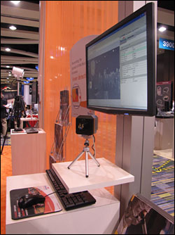
Xenics of Leuven, Belgium, had a number of its IR solutions on display at SPIE DS&S 2010.
Vida K. Simonaitis-Castillo of VKSC Consulting Inc. gave a lively talk on state-of-the-art crystal growth in the US. Until several years ago, she said, the US was at the forefront of crystal growth, but companies obtaining materials from other countries and federal procurement regulations such as export control issues have made it tough to get certain mission-critical materials from US sources. This, Simonaitis-Castillo said, could put a number of DoD programs in jeopardy. The path back to the forefront calls for consolidated multiagency funding and more research centers as well as ensuring crystal growth topics are taught in schools and universities.
In terms of telecom technologies, Gregory J. Whaley of Lockheed Martin Maritime Systems & Sensors discussed a project, part of the Air Force Highly Integrated Photonics program, in which he and his colleagues are developing an optically transparent, broadcast and select fiber optic network to be the next-gen interconnect for avionics platforms. The technology in development includes a tunable laser transmitter, a 32x32 port star coupler and a 32-port multichannel receiver.
And Paul A. Mitchell of Photonis USA Inc. presented a new optical receiver for high-speed communications. The new detector module is just as fast as a microchannel plate detector but has higher throughput; it also is three to five times faster than conventional photomultiplier designs. Data rates, Mitchell said, are expected to near 2 GHz.
Night vision systems and display technologies were popular topics, too; talk subjects ranged from novel night vision cameras to touch-screen and flat-panel displays, and even near-eye and head-mounted displays.
INVIS is an integrated night vision surveillance and observation system from TNO Defence, Security and Safety in the Netherlands. The system combines two digital image intensifiers and a thermal LWIR camera with a digital position information system that displays synthetic 3-D views of the environment. Noise reduction, resolution enhancement and natural color mapping techniques enhance the system's imagery.
And Opto Knowledge Systems Inc. discussed its prototype night-vision camera, which fuses a visible and near-infrared EMCCD camera with a longwave infrared microbolometer.
New products
In a Monday evening special session, hardware and software vendors gave brief presentations on new products, applications and practices in thermal imaging. Organizers said the event started five years ago, and has been popular and well-attended. From new imaging systems with precision-correlated data to new hyperspectral imaging cameras, from a new microbolometer to an uncooled thermal imager, from low-power thermal imaging to new IR cameras that expanding the spectral range, from new lens developments to new imaging developments that covering the full IR spectrum, company representatives gave early arrivals to the conference a sneak peek at the products that would be featured at the exhibition.
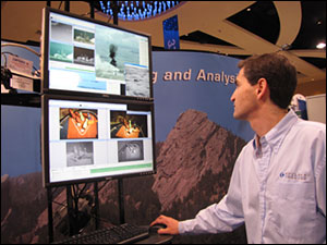
Carlos Jorquera, CEO of Boulder Imaging Inc., demonstrates the company's new Quazar 4.0 platform. The new Quazar can correlate uncompressed data from any kind of camera with input from any other system in real time.
As for the new products that were on display at the show, they ran the gamut of technologies and applications.
* Boulder Imaging Inc. of Louisville, Colo., released the latest version, 4.0, of its Quazar digital video recording software platform. CEO Carlos Jorquera and the Boulder crew had a fun demonstration set up, showing off the system's ability to correlate completely uncompressed data from any camera (analog, digital, even sonar, lidar or radar) with input from any other system. And it can do so in real time. "We're talking terabytes of data," said Jorquera.
* Sarnoff Corporation of Princeton, N.J., was showing its Acadia II visual processing system-on-a-chip. The Acadia II offers real-time, portable vision processing -- enhancement, stabilization, multisensor fusion and tracking - and system control with low power consumption.
* Sofradir EC of Fairfield, N.J., was showing a number of its new products, including the SSC R&D cameras, a new line of midwave and longwave infrared cameras for scientific, engineering and laboratory applications. Another new product from Sofradir EC was the Atom IR, which the company bills as the world's smallest thermal imaging model for OEM military products; its small, uncooled IR core makes it suitable for size-constrained night vision applications. Company rep Brooke Herbst said that both products garnered a lot of interest at the show.
* Genia Photonics of Lasalle, Québec, Canada, was showing its new synchronized tunable programmable lasers for various applications from biomedical to industrial. Defense applications include chemical sensing, Thz spectroscopy and mid-IR spectroscopy. The system synchronizes two lasers, one programmable laser and one MOPA (master oscillator power amplifier) laser. The average power is up to 100 mW per wavelength, and the synchronized mode tuning speed is up to 100,000 wavelengths per second.
* And Schott North America of Duryea, Pa., displayed its new LG-910 phosphate layer glass, an erbium-ytterbium-chromium doped phosphate based laser glass for diode and flashlamp pumped SSL systems. The applications include laser range-finding and dermatological uses.
Business opportunities
A panel of experts came together Wednesday afternoon to share progress and opportunities for businesses in US government programs.
Don D. Seeley, deputy director of the High Energy Laser Joint Technology Office, discussed what's in store for high-energy lasers in both research and application. He detailed a number of ongoing HEL projects and showed various video clips of laser test experiments. The HEL project is continuing, Seeley reported; JHPSSL has shown dramatic improvement; and RELI will lead to rugged and efficient technology.
Dr. David A. Honey, the director, research directorate, of the Office of the Under Secretary of Defense (AT&L), in the Office of the Director of Defense Research and Engineering (DDR&E), said the funding opportunities within his office focus on STEM education, high-performance computing, large data sets, cyber issues, environmental R&D and soft power.

Dr. Lisa Porter of the Intelligence Advanced Research Projects Activity agency discusses opportunities the agency offers to encourage the development of risky new ideas.
Dr. Lisa Porter of the Intelligence Advanced Research Projects Activity (IARPA) agency was the first to speak. The IARPA director from the Office of the Director of National Intelligence provided an overview of the agency and its focus on risky, nonimmediate research. "We only want the best and the brightest," she emphasized, noting that it doesn't matter who an applicant is, or whom he or she knows — what matters is the proposed idea and its credibility.
Ideas certainly took center stage this week at DS&S, from new research ideas to new products that once were merely the buds of ideas.
Laura Marshall, managing editor, Photonics Spectra
[email protected]