The rigors of research and measurement demand imagers that can capture data at extreme speeds and in ultralow light.
HANK HOGAN, CONTRIBUTING EDITOR
Scientific applications push imaging to the extremes. They demand cameras that can capture events as they unfold over nanoseconds, or capture processes that produce only a few photons across a broad spectrum — or a combination of both. In all instances, scientists require quantifiable data that can either prove or disprove a hypothesis.
Advancements in CMOS imaging technology have enabled scientific CMOS (sCMOS) sensors that, unlike their conventional brethren, enable cameras that offer some combination of low readout noise, higher resolutions, higher frame rates, and higher dynamic ranges.
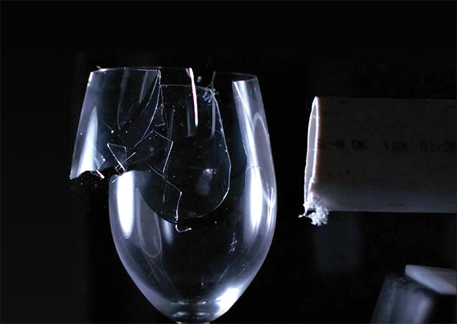
Imaging at speeds above 75,000 fps captures breaking glass. Courtesy of Vision Research.
These CMOS advancements arise, in part, from consumer demands, particularly in the smartphone market, said Stephanie Fullerton, life science marketing manager for Hamamatsu. “People want to take a perfect picture in low light or [capture] blur-free action pictures. That led to continuous advances in CMOS fabs and new product development.”
As a consequence, scientific cameras use advanced imaging sensors that often come from the same factories as consumer- and industrial-grade CMOS sensors. Gerhard Holst, head of the research and science department at Excelitas PCO, said, “There’s no special secret material combination, just a clever pixel architecture.”
Accelerating imaging
Ultrafast imaging is often used in research applications such as combustion or crash test studies, advanced microscopy, particle image velocimetry, and single-cell flow cytometry. But how fast is ultrafast? It depends, in part, on the application, as well as on the performance thresholds of current technology.
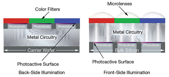
CMOS image sensor architectures. Back-side illuminated sensors improve the fill factor of photosensitive areas to enhance performance for scientific imaging (left). Courtesy of Teledyne Photometrics.
Excelitas PCO, for example, offers a line of cameras with exposure times as short as 2.5 ns. The cameras incorporate an image intensifier tube consisting of a photocathode, a microchannel plate, a phosphor screen, and a sCMOS sensor to image the screen. Incoming light creates a multitude of voltage-accelerated electrons that cause the screen to flicker, thereby enabling nanosecond imaging.
“If you know how to switch high voltages extremely fast, you can create extremely short exposure times,” Holst said. The company’s camera technology is used to study simulations of space debris as it hits objects or to observe high-voltage fuses at work.
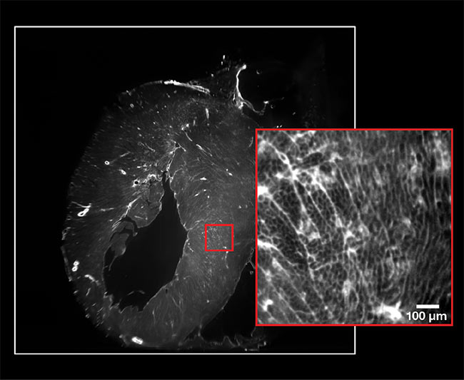
Light-sheet microscopy images an entire heart in a single acquisition. The camera’s full field of view (white square). The resolution at 2× magnification (red square).
CMOS sensor designers continue to evolve the technology to capture faster events. Case in point, Vision Research AMETEK’s TMX 7510 camera incorporates a custom CMOS sensor, along with other features, to allow the megapixel camera to achieve speeds of up to 75,000 fps — triple the speed that was previously possible, according to Kevin Gann, division vice president of research and development for the company. “It’s the first large-format, high-speed imaging sensor that’s made with back-side illumination,” he said.
In such high-speed applications, sensors face diverse challenges. First, they are photon starved due to short exposures. Without image intensification, pixels need to be large — approximately 10 or 20× the size of the 1.5-µm pixels found in a smartphone. Second, electronics on the sensors must move data off the chip as part of the imaging process. Minimizing the time needed for this readout requires the metal and other conductive traces on the chip to be larger. With traditional front-side illuminated imaging chips, these metal traces sit over the sensor’s photosensitive areas, blocking some of the light. Back-side illumination designs eliminate this conflict by placing the metal traces on one side of the chip and the photosensitive areas on the other.
One benefit of back-side illumination designs is the higher fill factor of their photosensitive area, which Gann said is almost 100%. As a result, pixel size in
Vision Research’s sensor is 18.5 µm, which is significantly smaller than its predecessor’s 28-µm pixel size.
Teledyne Photometrics also uses a back-side illumination design for its
Kinetix cameras, which have 6.5-µm pixels in 10-MP array sensors, said the company’s content manager and applications specialist Matthew Köse-Dunn.
The cameras operate at speeds of up to 500 fps at a 5 GB/s capture rate.
This speed, he said, is roughly 7× faster than is typical for sCMOS sensors at a 2K array size. But the acquisition speed can be greater with regioning, which crops the array to reduce the number of active pixels.
“When the sensor halves in size, the speed doubles,” Köse-Dunn said. “So, while the Kinetix is 500 fps at the full 3200 × 3200 pixel array, it will operate at 1000 fps at 1600 × 3200, and so on.”
At a 10 × 3200 array size, camera frame rates can top 100,000 fps, making it possible to image very short-lived events. Köse-Dunn said fluorescence correlation spectroscopy is an example of such applications.
A 3D image of a kidney captured using light-sheet microscopy. Courtesy of Hamamatsu. Courtesy of Excelitas PCO.
In its high-speed configuration, the Kinetix camera operates in 8-bit mode. The resulting 256 intensity levels match up well with most fluorescence signals. The cameras also can run in 16-bit mode, capturing 65,536 intensity levels, which results in a high dynamic range.
Gann predicts that further sensor advancements in the future will enable higher speeds, lower noise, and greater sensitivity, which will translate into cameras that are able to image even faster events. He also forecasts the increasing use of global shutter designs that will affect all of the pixels on a sensor simultaneously. Many low-noise applications today use a rolling shutter that, for fast moving events, may lead to motion artifacts because some pixels continue to collect light after others stop.
When photons are few
While the rapid shutter speeds in high-speed imaging can starve sensors of photons, other applications that use microscopes or telescopes face a scarcity of photons even at slower capture speeds. A sensor’s noise floor becomes an issue in such ultralow-light applications because it can obscure the signal. Advancements have lowered sCMOS noise levels to the point at which these sensors have become the preferred technology over electron-multiplying charge-coupled devices (EMCCDs), Köse-Dunn said.
Teledyne Photometrics maximizes
incoming photon capture and the resulting signal for its sCMOS sensors by leveraging back-side illumination designs. The result is a 95% quantum efficiency at peak wavelength.
Since the company’s sCMOS sensors are fast and sensitive, their exposure times can be significantly shorter, which, in turn, helps to minimize dark noise. Software algorithms, meanwhile, counter the sensor’s photon shot noise. These enhancements maximize sensitivity, which is key to capturing low light signals, Köse-Dunn said.
The uniformity and consistency of each pixel’s response is particularly important in scientific imaging because researchers rely on the pixels’ output in order to make accurate measurements and quantify experimental results, Hamamatsu’s Fullerton said. A fluorescent dye may blink on or off in response to a biological event, for example, but if a pixel erroneously does the same thing because its response is inconsistent, it could skew results.
Released in May 2021, Hamamatsu’s ORCA-Quest 9.4-MP camera’s sensor
enables a low read noise, low dark current, high quantum efficiency, sensor uniformity, and advanced pixel-level dark offset and gain calibrations. The sensor can be actively cooled to −20 °C. The
signal that comes off the camera is initially converted from a voltage to a digital number. An onboard field-programmable gate array then converts the digital number to a photon number.
“You can actually put it into a mode that will allow you to resolve individual photoelectrons. You can count them, up to about 200. That’s never been done before,” Fullerton said.
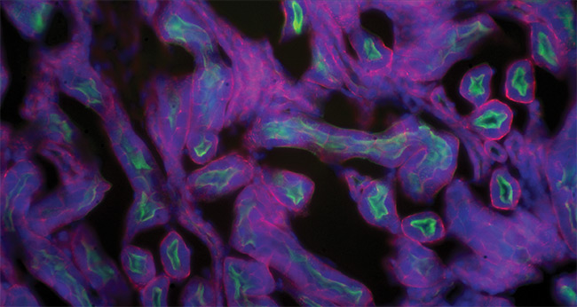
A section of a mouse kidney shows a composite of three stains: Alexa Fluor 488 wheat germ agglutinin (WGA) (green), Alexa Fluor 568 phalloidin (red), and DAPI (4′,6-diamidino-2-phenylindole) (blue). Courtesy of Excelitas PCO.
This photon number resolution is possible, in part, because of a read noise below 0.3 e− rms. Because the digitizer speed affects read noise, getting to that level requires paying careful attention to pixel design and lower readout rates.
However, even in normal operation, the read noise is half an electron. The ORCA-Quest’s speed is 120 fps at 9.4 MP with a 16-bit resolution, per the camera’s specifications. Fullerton said that life
science researchers may want camera speed that captures fast processes, such as the firing of neurons. But fast capture speeds even help for slower processes
because many cells and tissues cannot tolerate intense light. Keeping exposure times short by using a highly sensitive camera minimizes the harmful impact of light.
Excelitas PCO also makes scientific cameras with subelectron noise. The company’s pco.edge 10 bi CLHS camera, released in October 2021, has a 10.5-MP sCMOS image sensor with 4.6-µm pixels, and it delivers speeds of up to 120 fps. It specifies a 0.8-e− noise figure at lower frame rates due to a combination of a unique pixel architecture and thermal stabilization at low temperatures via active cooling.
Cameras with passive cooling tend to be more compact, Holst said, but they offer slightly worse noise performance than those with active cooling. And he said the choice of cooling method depends on performance requirements.
Applications for these fast, sensitive cameras, according to Fullerton, include light-sheet microscopy, where the cameras increasingly serve as research tools in clinical settings. In this microscopy method, systems illuminate specimens one plane at a time using a sheet of light to produce a 3D image while minimizing light exposure.
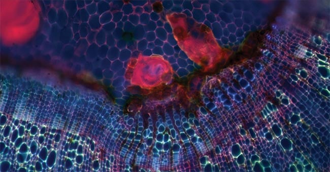
A stem slice of a Tilia species of tree or bush shows autofluorescence in three spectral ranges, indicated by three colors.
Another emerging application for sCMOS cameras involves genetically encoded, voltage-sensitive dyes that are used to image neuronal activity on millisecond timescales. A camera using a subarray can achieve the 300- to 1000-fps rate that is desired for this application, but doing so sacrifices the wider field of view (FOV) required for looking at an entire population of neurons all at once. This constraint is likely to change as dyes get brighter
and cameras get faster, Fullerton said.
Discussing future technology and
application requirements, Teledyne
Photometric’s Köse-Dunn said sensors currently integrate into cameras that
attach to optics in microscopes. But
microscopes typically have at most a 30-mm FOV. Cameras and the sensors within them will therefore have to conform to this limitation.
This constraint may change, said Köse-Dunn. “Once larger-FOV microscopes come out, larger-FOV cameras will match up.”
Bright future
A low read noise that improves sensitivity in low-light situations can also benefit spectroscopy applications, which typically leverage the technique of binning across a column in a sensor array. CCD sensors were traditionally the choice for spectroscopy because CMOS sensor noise increases with binning. However, emerging sCMOS technology minimizes this issue.
“When you get the read noise down really low, the penalty for binning is a lot less,” Fullerton said. “We could see CMOS move into more spectroscopy
applications.”
Other spectrum-related sensor innovations could also have an impact. In May 2020, Sony introduced a sensor that put shortwave IR-sensitive InGaAs atop a CMOS pixel. The result is an imager with a response that runs from the bottom of the visible range at 400 nm to 1700 nm in the shortwave infrared band. SWIR light penetrates tissue to a greater depth than visible light, making the band useful for gathering data without stressing living organisms such as laboratory mice.
The consensus among the experts interviewed is that scientific imaging technology will continue on a trajectory toward lower noise, higher acquisition rates, and wider spectral responses. One way to achieve these improvements, Holst said, is by using stacked sensors. In this architecture, pixels incorporate a local buffer that stores data temporarily. This approach makes it possible to collect image information at a high rate while avoiding added crosstalk noise and other performance penalties.
The experts also predict that conventional CMOS sensors will increasingly achieve the performance needed for many scientific imaging applications, thereby enabling applications on readily available equipment — for example, performing advanced microscopy using a smartphone for image capture.
“If you want a camera for a measurement — a reliable measurement — you have to plan properly,” Holst said. “Always, the application defines the requirements for the camera.”