Nadya Anscombe, Contributing Editor
Ask today's physics graduates if silicon can produce stimulated emission and show optical gain, and most would say no. But students graduating in the next few years will enter into an optoelectronics industry that has achieved the seemingly impossible: a silicon laser.
Silicon microphotonics has boomed in the last few years. Many silicon-based devices have
been demonstrated: waveguides, tunable optical filters, fast switches, fast optical
modulators, fast CMOS photodetectors, photonic crystals and microelectromechanical
systems. But not a laser. A silicon laser would, for the first time, allow monolithic
integration of photonics and electronics to share the same chip.
Despite huge research efforts by groups around
the world, a silicon laser — the device that promises to revolutionize the
optoelectronics industry — remains elusive. However, many researchers have
made silicon-based LEDs and a few have shown gain.
The most interesting aspect of silicon
laser research is that no two teams are developing the same technology. Each is
trying different and novel approaches in an attempt to squeeze light out of silicon.
Groups at the Università di
Trento in Italy and at the University of Rochester in New York are investigating
silicon nanocrystals and are the only ones to have reported gain; researchers at
the University of New South Wales in Sydney, Australia, have made an efficient
LED using bulk silicon and lessons learned from the photovoltaics industry; scientists
at the University of Neuchâtel in Switzerland are developing silicon-based
quantum cascade lasers; a group at Surrey University in the UK fired boron atoms
at bulk silicon to engineer local dislocations and make a relatively efficient LED;
at STMicroelectronics in Sicily, the only group to be backed by a large electronics
manufacturer is using silicon-rich oxide as a host for active ions; and another
team at the University of New South Wales is using porous silicon for the same purpose.
A laser host
Porous silicon was at one time thought to be the
answer to the quest for a silicon laser, but after several years of work, researchers
have been unable to increase the efficiency of light emission. This is why Mike
Gal’s group at the University of New South Wales is using porous silicon not
as a light emitter, but as the laser host that contains the optically active ions.
“We have already made a number
of very high quality porous silicon microcavities doped with erbium using ion implantation.
With better cavities, we think we will be able to get lasing in doped porous silicon
microcavities,” he said. “We think this will be a viable method to make
silicon lasers because, while we can make excellent optical microcavities out of
porous silicon, it is not an efficient emitter of light.”
And emission efficiency is the first
milestone in the race to develop a silicon laser.
The LED devices made by Salvo Coffa’s
group at STMicroelectronics hold the world record for efficiency. He and his colleagues used ions of rare-earth
metals such as erbium or cerium implanted in a layer of silicon-rich oxide —
silicon dioxide enriched with silicon nanocrystals 1 to 2 nm in diameter (Figure
1).
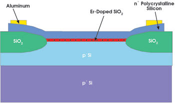
Figure 1. The LED devices made by Salvo Coffa’s group at STMicroelectronics hold
the world record for efficiency. His colleagues used ions of rare-earth metals such
as erbium or cerium implanted in a layer of silicon-rich oxide.
“Our device has an internal quantum
efficiency of 50 percent and an external efficiency of 10 percent,” he said.
The frequency of the emitted light
depends on the choice of rare-earth dopant — 1.54 μm for erbium —
and STMicroelectronics has patented techniques for implanting the rare-earth ions
in the silicon.
“It is important to get the correct
density of active ions and to ensure they do not cluster, or the optical properties
will be lost,” Coffa said. “It is also important to get a uniform electric
field across the device to prevent hot spots.”
The company has also patented a structure
in which two circuits, built on the same chip but electrically separated by insulating
silicon dioxide, communicate via optical signals using integrated silicon light
emitters and detectors. These devices will have numerous applications, including
motor control, power supplies, solid-state relays and others where the power circuit
must handle much higher voltages than the control circuit does.
In the longer term, the company is
investigating optical data transmission systems as well as low-cost integrated devices
for dense wavelength division multiplexing. Although many applications use an LED
as a light source, silicon LEDs have slow switching times and some applications
need faster modulation. Coffa is confident that building a laser is the solution.
“We hope to have an optically pumped laser by July 2003 and an electrically
pumped laser by the end of 2003.”
Before Coffa’s work, the efficiency
world record for a silicon LED was held by Martin Green’s group at the University
of New South Wales.1 The group’s expertise is in developing photovoltaic cells,
not LEDs. “This is a classic example of learning from work in a related area,”
Coffa said. “Green and his colleagues have optimized absorption processes
and used ultrapure silicon. This means that, because of the absence of defects,
the carriers have no place to recombine and will eventually emit a photon.”
Green’s electrically pumped LED
uses bulk silicon and emits at 1.15 μm near room temperature (Figure 2). It
has an internal quantum efficiency of 10 percent and an external efficiency of 1
percent — approximately the same levels obtained from GaAs devices 10 years
ago.
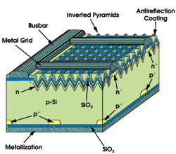
Figure 2. At the University of New South Wales, Martin Green’s
electrically pumped LED uses bulk silicon and emits at 1.15 μm at near room
temperature.
These efficiencies were obtained by
drastically reducing nonradiative recombinations. “We used small contact regions,
low-doped and extremely pure material, and the light extraction efficiency was enhanced
by texturing the surface,” Green said. High emissivity is obtained using inverted
pyramids on the top surface, formed by anisotropic etching. These pyramids not only
reduce reflection, but, more importantly, also increase emissivity by trapping weakly
absorbed light within the cell.
Observers of his work say that the
need for ultrapure silicon can be a disadvantage. But Green disagrees. “The
need for high-quality silicon is not such a big problem,” he said. “We
don’t work in a cleanroom, so I think the industry is capable of obtaining
the same quality standards that we have achieved.”
But he does not believe bulk silicon
will yield a laser. “I don’t think we will be able to get lasing in
bulk silicon because we need very high carrier densities. This is why we are going
to make 2-D structures. Due to quantum confinement effects, the bandgap increases
and emission at short wavelengths will occur. We expect to get photoluminescence
at 0.6 μm.”
The university has been granted a patent
for Green’s device and has provided funding for a high-throughput testing
laboratory. Using this approach, he hopes to have developed a fully functioning
optically pumped silicon laser in five years and an electrically pumped laser in
eight. And all this promising work has stemmed from research into photovoltaic cells.
Something to work with
“For many years the solar cell
industry has been taking advantage of the findings of the intense research done
by the world’s microchip industry to lower the cost and improve the efficiency
of solar cells,” Green said. “Even though we have been seeking quite
different results to those wanted by the microchip industry, we are all working
with silicon. Now we have turned the tables and given the microchip industry something
to work with.”
He said he was spurred to investigate
developing an LED when he saw a paper published by Kevin Homewood’s group
at Surrey University in the UK.2 The scientists claimed an external efficiency of
0.2 percent by using an approach very different from Green’s — introducing
localized defects that produce localized dislocation loops. This localization increases
the recombination rate of injected carriers. The resultant LED has a tunable wavelength
between 1.1 and 1.7 μm at room temperature.
Russell Gwilliam, a member of Homewood’s
group, said the main advantage of the approach is that “the technology is
100 percent CMOS-compatible and uses current fab tools in near standard process
windows.” He acknowledged, however, that there is still much work to do to
increase the efficiency and make a laser.
“As the light is generated within
the silicon, the external efficiency is reduced compared with oxide-based systems,
due to the relative refractive index of silicon compared with silicon dioxide,”
he said. “However, as a laser requires high internal reflection, this may
well work in our favor.”
Gwilliam is confident that his approach
will lead to a silicon laser. He has started a company, Si Light Technologies, to
commercialize the work and is looking for funding, he said. Of the other approaches,
he is most skeptical about silicon nanocrystals. “We investigated silicon
nanocrystals some years ago. We even patented the approach. But we could not get
sensible charge injection into the nanocrystals because they are based on silicon
dioxide. Our new silicon-based approach does not have these problems.”
Lorenzo Pavesi from Università
di Trento, whose work is based on silicon nanocrystals, acknowledged that charge
injection may be a problem. “But we have demonstrated that silicon can show
optical gain, whereas the Surrey group has not yet been able to do this,”
he said.
Like Homewood and Gwilliam, Pavesi
published his work in Nature and raised the awareness of silicon-based LED and laser
research.3 Pavesi’s optically pumped device emits from 750 to 900 nm, and
some of the devices made by the group have an external efficiency of 1 percent (Figure
3).
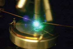
Figure 3. Lorenzo Pavesi at the Università di Trento in Italy has demonstrated that
silicon can show optical gain.
“There are still materials issues
to be faced,” he said. “Electrical pumping may be a problem.”
Philippe Fauchet at the University
of Rochester agrees. His group has made silicon LEDs by layering amorphous silicon
with silicon dioxide and using an annealing process to turn the amorphous silicon
into an array of silicon nanocrystals. “The nanocrystal technique has one
inherent problem,” he said. “For it to work, we need to fabricate isolated
quantum dots, but this in turn means current injection will be poor, because the
nanocrystals are isolated from each other.” His group has shown “large
gain” and plans to present its findings at a materials conference that will
be held in April.
Silicon nanocrystals emit visible light
at room temperature, and the emission band depends on the mean size of the nanocrystals:
The emission band shows a blue shift and a narrowing as their size decreases. The
mechanism for this luminescence is still being debated, but Pavesi believes that
the emission originates in nanocrystals that are coated with a stressed silica
shell. This enhances the formation of interface oxygen-related states on the surface
of the silicon nanocrystals, which emit when excited.
Although this approach has been successful
for Pavesi, he said that not all the physics behind the technology is completely
understood.
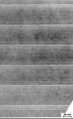
Figure 4. A transmission electron microscope captured five periods
of Jérôme Faist group’s quantum cascade silicon-germanium LED.
The light gray lines are the Si barriers, the dark gray lines are SiGe (80 percent
Ge) and, where the scale is indicated, SiGe (50 percent Ge). The small dots are
atoms. The thinnest Si barrier is only 4 Å (0.4 nm) thick. This shows the
group’s ability to grow SiGe layers with any Ge content with an extreme control
on the layer thickness.
Jérôme Faist at the University
of Neuchâtel, however, has the opposite problem. He has a system — the
quantum cascade laser — that is well-understood and that theoretically will
produce a laser with very high efficiencies (Figures 4 and 5). But, practically,
his group still has a long way to go before it demonstrates a laser.
The Neuchâtel device emits at
7 μm but works only at low temperatures. “We use very thin alternating
layers of silicon and germanium to confine carriers in a sandwich of layers,”
Faist explained. “They cascade through these layers, emitting a photon at
each step, like an electronic waterfall.”
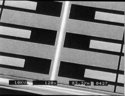
Figure 5. A scanning electron microscope captured this image of Jérôme Faist’s group’s LED. The white line is the waveguide, and along the waveguide are the top metal electrodes (dark gray). The light gray rectangles are the bottom electrodes. Most
of the black surface is a silicon-nitride insulating layer.
The group recently published a paper
showing electroluminescence from quantum cascade structures.4 In previous structures,
strain between the silicon and germanium layers was a big issue. But the scientists
have used strain compensation techniques on samples consisting of up to 50 periods
(about 700 quantum wells) and redesigned the active region. Using these devices,
Faist believes population inversion may be possible.
Enough power?
Population inversion is the next milestone in
the race to develop a silicon laser. But although all the aforementioned researchers
believe that population inversion — and therefore a laser — will be
possible, Coffa believes that there is one parameter that many have not considered.
“I am positive a silicon laser will be demonstrated soon, and, obviously,
I hope it is by my group, but the important question is whether such a laser will
emit enough power to be useful,” he said. “For an integrated application
with a very sensitive detector, nanowatts of power are sufficient. But for most
other applications, milliwatts of power are needed, and I am not sure if this can
be achieved by any of the groups working on a silicon laser.”
There are still many obstacles to overcome:
Output power, efficiencies, optical gain and radiative recombination rates need
to be increased if the silicon laser is to become a reality. But if one takes into
account that modern gas lasers operate with very low gain and modern solid-state
lasers have low radiation decay rates, the prospect of a visible silicon laser becomes
more realistic.
References
1. M. Green et al. (August 2001). Efficient silicon
light-emitting diodes. NATURE, p. 805.
2. K. Homewood et al. (March 2001).
An efficient room-temperature silicon-based light-emitting diode. NATURE, p. 190.
3. L. Pavesi et al. (Nov. 23, 2000).
Optical gain in silicon nanocrystals. NATURE, p. 440.
4. L. Diehl et al. (December 2002).
Electroluminescence from strain-compensated Si0.2Ge0.8/Si quantum-cascade structures
based on a bound-to-continuum transition. APPLIED PHYSICS LETTERS, p. 4700.
Why Is Silicon an Inefficient Light Emitter?
Silicon is an indirect bandgap material. Light emission is via a phonon-mediated process
with low probabilities: Spontaneous recombination lifetimes are in the millisecond
range. In standard bulk silicon, competitive nonradiative recombination rates are
much higher than the radiative ones, and more of the excited electron-hole pairs
recombine nonradiatively. This yields very low internal quantum efficiencies for
bulk silicon luminescence. In addition, fast nonradiative processes such as Auger
or free-carrier adsorption prevent population inversion for silicon optical transitions
at the high pumping rates needed to achieve optical amplification.