
Semiconductor Leaders Deploy NVIDIA Computational Lithography
SANTA CLARA, Calif., March 23, 2023 — According to NVIDIA, the computing company’s cuLitho software library for computational lithography is being integrated by leading players in the semiconductor industry. The technology serves to accelerate design and manufacturing of next-generation chips, as current production process are nearing physical limits.
The software library is being integrated by Taiwan Semiconductor Manufacturing Co. (TSMC), NVIDIA said, as well as by Synopsys, which is integrating the library into its software, manufacturing processes, and systems for the latest-generation NVIDIA Hopper architecture GPUs. ASML is also working closely with NVIDIA on GPUs and cuLitho, and it plans to integrate support for GPUs into all of its computational lithography software products, NVIDIA said.
The advancement enables chips with smaller transistors and wires than are currently achievable while accelerating time to market and boosting energy efficiency of data centers that run 24/7 to drive manufacturing processes.
The advancement also lays the foundation for 2 nm and beyond, according to NVIDIA founder and CEO Jensen Huang.
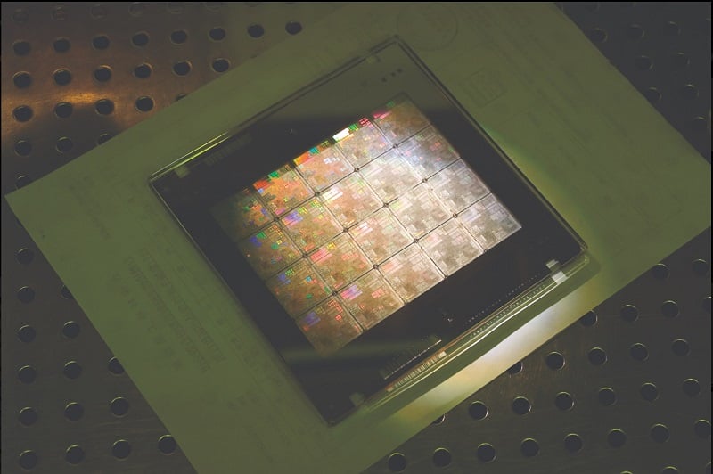
NVIDIA’s cuLitho software library significantly boosts potential outputs and efficiency of computational lithography processes. Courtesy of NVIDIA.
Running on GPUs, cuLitho provides performance improvements up to 40× times beyond current lithographic capabilities, accelerating massive computational workloads that currently consume tens of billions of CPU hours each year. The software allows 500 NVIDIA DGX H100 systems to achieve the work of 40,000 CPU systems, running all parts of the computational lithography process in parallel, reducing power needs and potential environmental impact.
In the near term, fabs using cuLitho could produce 3 to 5× more photomasks per day using 9× less power than current configurations. A photomask that previously required two weeks can now be processed overnight.
Longer term, cuLitho will enable better design rules, higher density, higher yields, and AI-powered lithography.
“Our collaboration with NVIDIA on GPUs and cuLitho should result in tremendous benefit to computational lithography, and therefore to semiconductor scaling,” said Peter Wennink, CEO of ASML. “This will be especially true in the era of high NA extreme ultraviolet lithography.”
A fab process change often requires an OPC revision, which creates bottlenecks. Now, according to NVIDIA, cuLitho helps to remove these bottlenecks and makes possible novel solutions and innovative techniques such as curvilinear masks, high NA EUV lithography, and sub-atomic photoresist modeling needed for new technology nodes.
/Buyers_Guide/ASML/c25112
/Buyers_Guide/Synopsys_Inc_Optical_Solutions_Group/c10902