Breakthroughs in CMOS fabrication techniques promise lower-cost sensors that are capable of detecting light in the lower end of the SWIR spectral region.
MATTHEW DYSON, IDTECHEX
Image sensors are part of every smartphone and may seem to be a ubiquitous, mature technology — however, this is far from the case. While conventional CMOS detectors for visible light are well established, extensive opportunities exist for more complex and innovative image sensing hardware to offer capabilities beyond simply acquiring the intensity values at each pixel.
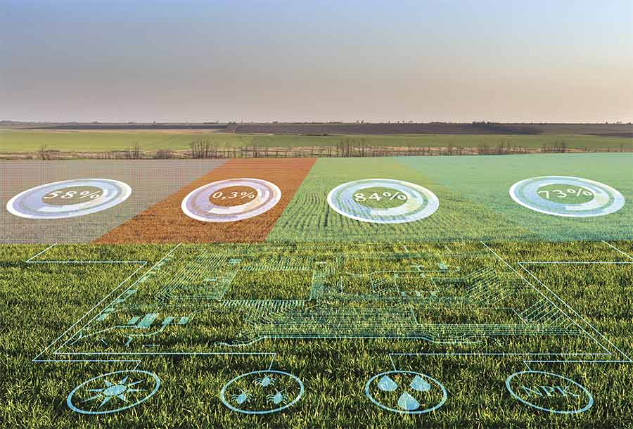
Precision farming promises increased agricultural yield by enabling plants to receive targeted fertilizer and pesticide treatments. Algorithmic image analysis can help to discern differences in leaves or fruit at different stages of ripeness. Increasingly, SWIR imaging is also used in cases where visible light cannot reveal substantial differences. Courtesy of iStock.com/Igor Borisenko.
These opportunities largely stem from the ever-increasing adoption of machine vision, in which image analysis is performed by computational algorithms. Machine learning requires as much input data as possible to establish correlations that can facilitate object identification and classification. Therefore, acquiring optical information over various wavelength ranges — or with spectral resolution, for example — is highly advantageous.
Expect to see InGaAs alternatives for SWIR imaging, event-based vision, and even thin-film photodetectors appearing in consumer devices over the next five years.
Of course, emerging image sensor technologies offer many other benefits, such as enabling SWIR imaging at a lower cost than existing approaches, increased dynamic range, improved temporal resolution, spatially variable sensitivity, high-resolution global shutters, reduced scattering, and flexibility/conformality. These emerging technologies can also be applied across a very wide range of applications in many different sectors1.
Autonomous vehicles
Ever-increasing levels of vehicle
autonomy are poised to revolutionize both personal and freight transport, reducing the time that vehicles spend sitting in traffic, and ushering in new transportation modes such as robo-taxis. Of course, autonomy requires that vehicles can always obtain a clear picture of their surroundings, with multiple sensors providing redundancy. This sensor fusion process includes lidar and radar along with cameras.
While much of the technological discussion centers on lidar, extensive opportunity also exists to use other
innovative image sensing technologies,
such as SWIR imaging. Given the high price of indium gallium arsenide (InGaAs) sensors, motivation is considerable to develop much lower-cost alternatives that can detect light toward the lower end of the SWIR spectral region. Such SWIR sensors could then be employed in vehicles to provide better vision through fog and dust, due to the reduced scattering of light at longer wavelengths (Figure 1).
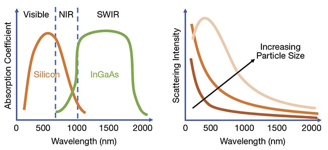
Figure 1. Conventional silicon detectors cannot detect light with wavelengths above ~1000 nm (left). Currently, indium gallium arsenide (InGaAs) is used to image in the SWIR region, but its high price leaves room for emerging technologies. An advantage of SWIR imaging is reduced scattering from many different particle sizes (right), enabling cameras to see farther through conditions such as fog and dust. Courtesy of IDTechEx.
One way to achieve affordable SWIR imaging is to extend the sensitivity of silicon photodetectors beyond the usual 1000 nm by increasing their thickness and structuring their surface. Since this extended silicon approach can utilize existing CMOS fabrication technologies, it is likely to be a durable and relatively low-cost alternative that
is highly applicable to autonomous
vehicles and advanced driver assistance systems (ADAS). However, since this method is based on silicon, it is best suited for detecting light toward the lower end of the SWIR spectral region.
Another technique that will likely be more expensive than the extended silicon approach but that is capable of imaging at longer wavelengths involves using a hybrid structure that comprises quantum dots (QDs) mounted onto a CMOS readout integrated circuit. Quantum dots have highly tunable
absorption spectra that can be controlled by changing their diameter, enabling light up to 2000 nm to be absorbed. QD-on-CMOS hybrid detectors that can image up to 1700 nm are already commercially available. The ability to image at long wavelengths makes them especially promising for industrial imaging applications and hyperspectral imaging.
Another technology that is gaining traction for autonomous vehicles and ADAS is event-based vision (Figure 2). This approach relies on asynchronously detecting and recording changes in time-stamping intensity rather than capturing complete frames at a constant frequency. Relative to conventional frame-based imaging, event-based vision combines greater temporal resolution of rapidly changing image regions, with much reduced data transfer and subsequent processing requirements. Increased dynamic range is an additional benefit.
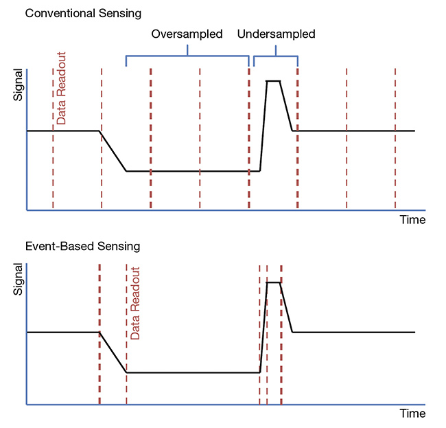
Figure 2. A schematic comparing conventional and event-based sensing. Note the higher temporal resolution enabled by event-based sensing, with fewer data readouts. Courtesy of IDTechEx.
UAVs require collision avoidance
Similar to autonomous vehicles, unmanned aerial vehicles (UAVs), or drones, require a wide range of sensing capabilities in order to establish their environment and avoid collisions. SWIR imaging is particularly important in UAVs because SWIR’s longer wavelengths reduce the scattering caused by water droplets in clouds.
UAVs are also a very promising market for event-based sensing, which rapidly identifies changes in the surroundings and hence helps to avoid collisions. A vision sensing technology
that lowers the image processing requirements — and therefore lowers power consumption — is especially desirable for a drone, given the need
for it to be as light as possible. Because of these benefits, some companies
are specifically developing software that supports UAV collision avoidance using data from event-based vision sensors.
Industrial inspection
Machine vision is already well established for use in industrial contexts, especially in object recognition and quality control. While many industrial tasks such as object identification or quality control can be performed via computational analysis of images
captured by conventional cameras, SWIR or hyperspectral imaging can obtain additional insights.
For example, the absorption band of water that peaks at around 1400 nm makes SWIR imaging especially good for distinguishing between water and other liquids. Furthermore, SWIR
imaging is good for distinguishing
between visually identical materials, due to its ability to identify variations
in reflection spectra in the SWIR region — enabling, for example, metal or stone contaminants in food to be identified.
The spectral resolution of hyperspectral imaging enables the detection of even more subtle differences in properties. Example applications include detecting the early stages of food decomposition and separating different plastics for recycling. Reducing the price of SWIR sensors using the emerging technologies outlined above will enable such capabilities to be more widely deployed.
Improving smartphone capabilities
High-quality cameras are an essential component of any smartphone. Flagship smartphone devices feature multiple cameras to enable wide-angle and zoomed images. However, at
present, all the image sensors are CMOS-based and primarily aim to detect visible light, although NIR light is used for face recognition.
Manufacturers are always looking for ways to differentiate their products by adding features to improve photography and video capabilities. One way to accomplish this is by adding event-based vision sensors, an approach
that PROPHESEE, a developer of computer vision solutions, has taken. The company announced that it had received a strategic investment from Chinese smartphone manufacturer Xiaomi in July 2021.
A key motivator for adding event-based vision to smartphones is to
correct motion artifacts computationally by utilizing the high temporal resolution of event-based sensors. Facilitating slow-motion video is another benefit. With conventional image sensors,
slow-motion video requires a very high frame rate (i.e., >100 fps), which produces huge amounts of data. Combining an event-based sensor with a conventional image sensor enables sampling of the image at a much lower rate (i.e., 10 to 20 fps), since the event-based data can be used to interpolate between frames. This methodology, which is still under development, can produce slow-motion video at the equivalent of 200 to 300 fps, while requiring only about 10% of the data storage.
Another potential development, albeit one that is only likely to unfold well
into the future, involves incorporating hyperspectral (or at least multispectral)
image sensors into smartphones.
The cosmetics and skin care industries
employ hyperspectral imaging to detect subtle variations in skin tone and health, and the technology could be further used to tailor product suggestions
for individual customers. Currently, hyperspectral imaging is only available in-store, but incorporating hyperspectral cameras into smartphones or webcams could enable sophisticated product selection to take place at home.
Precision agriculture
Precision farming promises to increase agricultural yields by enabling individual plants, or at least regions of a planted field, to receive targeted fertilizer and pesticide treatments. Furthermore, planting and harvesting could be tailored to ground conditions in a particular area and to the status of a particular fruit or plant.
Clearly, such targeting requires careful analysis of the individual plants or regions of the field. While this can be accomplished via algorithmic image analysis, conventional cameras in the visible spectrum cannot always identify subtle differences between leaves or fruit at different stages of ripeness. SWIR imaging resolves this challenge because surfaces that look similar under visible light can show substantial differences under SWIR light (bruised fruit is an excellent example). Also, SWIR’s reduced scattering effects facilitate imaging in otherwise adverse conditions, such as fog. Currently, the high price of InGaAs sensors limits their adoption, but emerging image sensor technologies, such as extended-range silicon photodiodes and QD-on-CMOS hybrid detectors, should bring costs down.
Additional insight into plant health can be gained via hyperspectral imaging. Rather than expressing an image as red, green, and blue (RGB) values
at each pixel location, hyperspectral imaging instead records a complete spectrum at each point, creating a full 3D data set. Recording hyperspectral images requires that a dispersive
element, such as a prism or diffraction
grating, project a single line onto a 2D image sensor. Since a complete reflection spectrum is obtained for each pixel, far more information can be gained from a hyperspectral image than from a standard image, enabling supervised machine learning to quantify chemical composition more precisely and hence to determine ripeness or disease.
Direct x-ray imaging
Medical x-ray imaging provides a good example of how sensor innovation is poised to fundamentally change the detector form factor, as well as to improve sensitivity and spatial resolution. At present, digital x-ray detectors typically require a scintillator layer — such as cesium iodide (CsI), which converts incident x-ray photons into lower-energy visible photons — mounted atop a silicon photodiode. This architecture results in heavy, bulky sensors, and spatial resolution is limited by the isotropic reemission from the scintillator layer.
An exciting alternative that offers both improved sensitivity and improved
spatial resolution is direct x-ray detec-
tion using thick (multiple-micron) semi-
conducting perovskite layers (Figure 3). Organic-inorganic hybrid perovskites, such as methyl ammonium lead halide (MAPI), have been making headlines over the last few years for rapidly increasing photovoltaic quantum efficiency. Single-junction solar cell efficiency has recently reached as high as 25%. Additionally, hybrid perovskite materials are being investigated for use in thin-film photodetectors and LEDs.
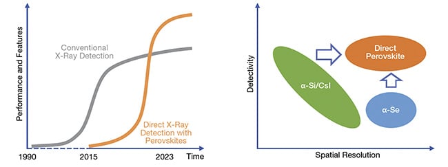
Figure 3. The introduction of perovskite-based direct x-ray sensors will improve the overall detection performance versus conventional x-ray detection (left), ending the existing need to compromise between detectivity and spatial resolution (right). Courtesy of IDTechEx.
In direct x-ray sensors, the heavy lead ions within the perovskite films attenuate the x-rays and generate charges that are then extracted via the electrodes. The lack of a separate scintillator layer improves spatial resolution because the location of incident x-rays is measured directly.
The technology is being developed via a collaboration between Siemens Healthineers and Holst Centre, a Dutch research center that develops technologies for printed and flexible electronics. The technology is discussed in detail in a recent open-access paper published in Nature Electronics2. Currently, the detector is an early-stage prototype and measures only a few centimeters across, but the plan over the next few years is to scale it to the size of a 20- × 20-cm panel, after which it will enter product development and qualification.
Thin, flexible biometric imaging
During customs procedures at airports, officials often take a full set of travelers’ fingerprints, since this is much more secure than imaging just a single print. At present, digital fingerprint readers that are capable of imaging all four fingers simultaneously are bulky and costly because reflections from each finger must be focused onto a small silicon photodetector. Therefore, simultaneous measurement of multiple fingerprints is currently largely restricted to niche applications.
Large-area thin-film photodetectors
that utilize solution-processable semiconductors offer a solution to this challenge by eliminating the need for light to be focused. Organic photodetectors have a similar structure to organic photovoltaic cells, comprising a bulk heterojunction of materials with an energy-level offset sandwiched between electron and hole transport layers. Transparent conductive films form the electrodes. The conductive polymer PEDOT:PSS is commonly used if flexibility is required.
Along with fingerprint capture, thin-film photodiodes are highly suitable for biomedical applications in which flexibility adds a significant benefit. Researchers have conducted clinical trials of pulse oximeters that use thin-film photodiodes, which could enable conventional bulky thumb clips to be replaced with more comfortable skin patches. Larger-area thin-film photodetectors have also been used to image blood vessel structure through the skin via a detector wrapped around a limb.
Large-area organic photodetectors (OPDs) are being developed by French company ISORG, with the target application of biometric imaging, including underneath smartphone screens. Perovskite photodetectors (PPDs) are an emerging alternative to OPDs that promises lower material costs and potentially higher detectivities3. Although still in the R&D stages and many years away from commercialization, PPDs not only promise cheaper materials and higher detectivity due to reduced dark current but also higher cut-off frequencies due to rapid charge extraction.
Substantial opportunities exist across multiple application sectors for a range of emerging image sensing technologies that offer capabilities beyond conventional CMOS sensors (Figure 4). These opportunities are driven by the increased use of machine vision and automation, along with a desire to bring imaging capabilities that are currently only available in the laboratory to a much wider audience. Expect to see InGaAs alternatives for SWIR imaging, event-based vision, and even thin-film photodetectors appearing in consumer devices over the next five years.
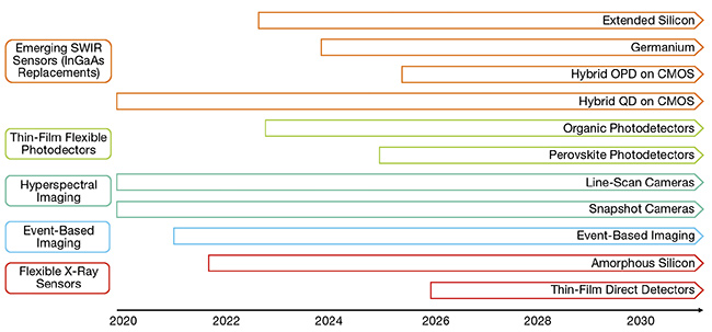
Figure 4. An adoption roadmap for a wide range of emerging image sensor technologies. The forecast date of first mainstream adoption for a specific application (start of arrow), excluding R&D, trials, and prototyping. OPD: organic photodetector; QD: quantum dot. Courtesy of IDTechEx.
Meet the author
Matthew Dyson, Ph.D., is a senior
technology analyst at IDTechEx. He specializes in image sensors and printed, organic flexible, and hybrid electronics. Dyson received a doctorate in physics from Imperial College, where he investigated the optoelectronic
properties of organic semiconductors. His post-doctoral work focused on organic photodetectors. At IDTechEx, Dyson analyzes technical innovations, applications, and commercial opportunities across the image sensor and the printed, organic flexible, hybrid landscape. He is based in London.
References
1. IDTechEx (2021). Emerging image sensor technologies 2021-2031:
applications and markets.
2. S. Deumel et al. (2021). High-
sensitivity high-resolution x-ray
imaging with soft-sintered metal
halide perovskites. Nat Electron, Vol. 4, pp. 681-688, www.doi.org/10.1038/s41928-021-00644-3.
3. R. Ollearo et al. (2021). Ultralow dark current in near-infrared perovskite photodiodes by reducing charge injection and interfacial charge
generation. Nat Commun, Vol. 12, No. 7277, www.doi.org/10.1038/s41467-021-27565-1.