Making and inspecting semiconductor chips requires pushing laser
techniques deeper into the ultraviolet.
Hank Hogan, Contributing Editor
As semiconductor feature sizes shrink, manufacturers need a light touch — and at the right wavelength. A look at three areas — lithography, metrology and assembly — shows how photonics-based innovations are tackling some of the semiconductor industry’s most pressing problems.
Steppers are among the most critical tools used for semiconductor manufacturing and are at the heart of the photolithographic process, which transfers the features that are on a mask onto the photoresist material on a wafer. Subsequent processing reproduces that transferred layout in layers of conductors and insulators that eventually comprise a functioning integrated circuit. Today, state-of-the-art features are as small as 65 nm. Soon, they will be 45 nm, and the generation beyond that, 32 nm. The latter two scales are several years away, although the equipment needed for them is being rolled out now.
Although designed for manufacturing on a microscopic scale, the latest lithography stepper lens from Carl Zeiss SMT AG of Oberkochen, Germany, is not small. The Starlith 1900i weighs more than a metric ton, stands several feet tall and is as big around as a tree trunk. A catadioptric lens consisting of reflecting mirrors and refractive optics, it enables volume semiconductor production at 40-nm resolution, according to the company.
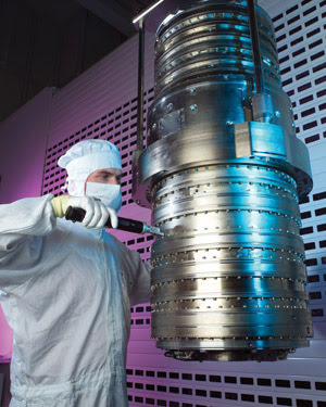
The device pictured is a catadioptric lens that, according to the manufacturer, can achieve 40-nm-resolution lithography on semiconductor chips. Courtesy of Carl Zeiss SMT.
The stepper lens has a numerical aperture of 1.35 and is intended for use in immersion lithography, a technique that replaces the air gap between wafer and stepper with water or another fluid. Wolfgang Rupp, Zeiss’ vice president of systems for the lithography optics division, noted that the device is, in some sense, end of the art. “Without compromising the field size, an NA of 1.35 is the practical limit for water-based immersion systems.”
Even reaching that practical limit required quite a bit of engineering. Besides the optical techniques, the company had to employ stringent manufacturing methods. Rupp said that several of the lens elements required precision surfaces at the scale of a few atoms, while manufacturing had to be done in particle-controlled cleanrooms under strict environmental conditions. The company recently invested h450 million (about $573 million) in a new factory to build products such as the 1900i lens.
Although such lenses are essential, another key stepper component is the laser. For example, Cymer Inc. of San Diego is scheduled to go into production soon with the XLR 500i, a 60-W ArF pulsed excimer laser that operates at 193 nm and that is intended for use in 45-nm immersion lithography.
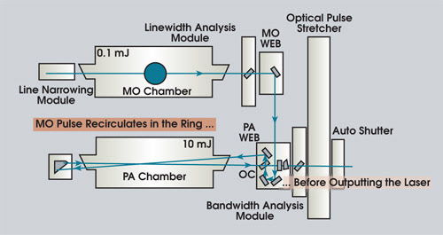
Cymer Inc. manufactures a 193-nm pulsed excimer laser for use in immersion lithography. The device features an internal optical architecture in which power in the master oscillator (MO) is balanced with that in the power amplifier (PA).
What distinguishes this laser from its predecessor is its internal optical architecture, according to Cymer’s vice president of technical marketing, Nigel Farrar. In both generations of the laser, the output from a master oscillator feeds into a power amplifier before exiting through an optical pulse stretcher. In the newer device, however, the power in the master oscillator is decreased by a factor of 10 to about 0.1 mJ, whereas the power amplifier is upped by the same factor.
“It is distributed differently over time, but the output of the pulse energy remains the same,” he said.
What this rebalancing of power does, he noted, is provide better performance. The lower power levels in the master oscillator lead to roughly a doubling of its lifetime. That cuts operating cost and increases availability because of decreased downtime. In addition, the power amplifier operates in saturation, which increases pulse stability by a factor of 1.5. A more stable pulse energy will lead to greater dose stability, permitting the laser to be fired fewer times per exposure while providing tighter critical dimension control.
Working in reverse
These hardware developments seek to extend optical lithography and make it more economical. Luminescent Technologies Inc. of Palo Alto, Calif., is tackling a different aspect of the problem. Because of diffraction, photoresist limitations and other effects, the features on a mask are not precisely printed on a wafer; for example, right angles tend to become rounded, especially on inner corners.
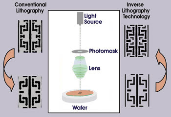
Diffraction and photoresist limitations can result in imprecise mask features. One approach to the problem is to invert the standard technique — using algorithms that start with the pattern as it should appear on the wafer and then creating the appropriate mask layout. Courtesy of Luminescent Technologies Inc.
The standard solution is to use optical-proximity correction, which adds rectangles and other features to the mask so that the image as printed on the wafer more closely resembles the ideal. Andrew Moore, a scientist and vice president of business development for North America and Europe at Luminescent Technologies, noted that this is a trial-and-error approach that starts with the mask and adjusts it. In contrast, he said, the company’s approach is to solve the inverse problem by using algorithms that start with the pattern as it should appear on the wafer and then to create the appropriate mask layout, resulting, in theory, in the best mask layout.
Moore said that the technique involves some compromises because adding features increases the complexity and cost of the mask. However, those trade-offs do not involve a permanent loss of the structure data, as it should be on the mask to create what is desired on the wafer. “We always carry in our system the mathematically correct image. We know what it would be in an ideal case. In order to make it manufacturable, we simplify that.”
In practice, implementation of the inverse lithography technique adds stair steps to right angles, making them more curvelike. Phantom features appear between desired structures. These extra features arise in spots where the interplay of light and resist might otherwise create undesired objects on the wafer. Their addition prevents such objects from appearing.
Coming up with the inverse function requires extensive knowledge of the process because it involves the resist, the steppers and associated processing effects. For that reason, Luminescent Technologies enters into what Moore calls “deep partnerships” with its customers.
Looking for problems
Whereas lithography draws much of the attention, it is not the only semiconductor area in which lasers and other light sources are used. By some accounts, there are 20 to 40 inspection stations for every stepper. Resist patterns must be checked as well as the outcome of such follow-up processes as layer etching and resist stripping. Deposited films also must be measured and inspected.
David Rideout, product manager of the microimaging division at Olympus Industrial America of Orangeburg, N.Y., noted that the trend toward decreasing feature sizes is driving manufacturers to use shorter and shorter wavelengths. Optical constraints are forcing this move. Even with the ability to discard unwanted light and to optically section samples, a confocal microscope runs up against the diffraction limit. With a 408-nm light source, microscope resolution is limited to 120 nm in the X- and Y-axes. That figure is too large for the most critical features of 90- and 65-nm process nodes and will be too coarse for even more layers in the 45- and 32-nm nodes of the future. Because resolution is proportional with the wavelength of the light source, manufacturers are faced with two choices. “You are going to need either new imaging technology or much shorter wavelengths,” Rideout said.
Olympus has had a 248-nm inspection system available since 2003, although it does not use a laser for technical and economic reasons. Other manufacturers also are debuting UV inspection stations. In June 2005, for example, toolmaker Applied Materials Inc. of Santa Clara, Calif., introduced an inspection system with a 266-nm laser source.
In response to other inspection needs, Olympus recently unveiled a laser-based IR system that operates at 1310 nm. The advantage of IR, Rideout explained, is that it penetrates silicon. Thus, it can make measurements of buried layers, looking for gaps and alignment as well as checking on the effect of the extreme environmental conditions that often are used during accelerated life testing of a circuit.
The system can perform similar inspections on packaged parts, even those that have not been opened to expose the silicon encapsulated in the plastic. “It is a confocal laser, so it has very high resolution in X, Y and Z through the package,” Rideout said.
Fixing defects
Another company that is using both UV and IR sources is Electro Scientific Industries Inc. of Portland, Ore. Among other things, the company makes link-processing systems. These machines are used by memory manufacturers to repair products. Modern memory chips are designed with spare cells; normally inactive, spares replace defective cells, thereby correcting problems and improving yield. This swapping in and out takes place when conductive links are blown via laser and therefore are removed from the circuit.
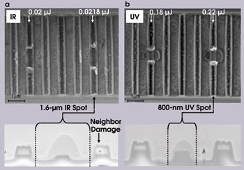
Repairing memory chips requires clean excavation of conductive links on the semiconductor material. Making links as small as possible requires short wavelengths. The images above show the differences between using an IR laser (A) and a UV laser (B) to create links. Courtesy of Electro Scientific Industries Inc.
The process must be fast — because millions of chips are manufactured annually — and clean — because debris showering down upon other parts of the die may lead to problems. It also must be done at progressively smaller sizes. As features on chips shrink, links also must shrink so that chips can become denser. Therefore, customers of companies such as Electro Scientific Industries want a smaller spot size.
Paul Kirby, a product manager at the company, noted that making smaller links implies a need for shorter wavelengths. Its older products used IR lasers at 1064 and 1340 nm; however, the company now is concentrating on UV sources, he said. It is empoying a 355-nm Nd:YAG laser in pulsed mode, shipping products built around this laser after making changes in its manufacturing process that were required by the more energetic UV photons.
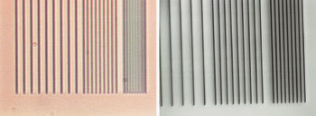
Because shorter wavelengths enable the imaging of smaller features, semiconductor toolmakers are forced to use UV sources as feature sizes shrink. These images of three sets of 120-nm-wide lines with aspect ratios of 1:1, 1:3 and 1:5, left to right in A and B, show the difference that wavelength choice makes. A 408-nm source was used to image the lines in A, whereas a 248-nm source was used to image the lines in B. Courtesy of Olympus Corp.
The company recently introduced a dual-head IR system with a single 1340-nm laser that is split into two beams. Having dual heads enables customers to gain throughput, with as much as a 90 percent increase possible over a single-beam system when the link layout is optimized. Kirby said that UV ultimately will be the way everyone will go, but that, in the meantime, the dual-head IR approach is the right one for some customers. “For the ones who have to stagger and group their fuses and come up with these other complex layouts, then the dual beam is perfect.”
Besides a shorter wavelength, the other trend that Kirby sees is increased repetition rate. A decade ago, pulse rates were 4.6 kHz in the company’s products. Today it is shipping 100-kHz systems. Although not translating directly into increased throughput, the faster repetition rates have upped machine productivity significantly.
The sweet spot
Neither a semiconductor manufacturer nor a toolmaker, Deep Photonics Corp. of Corvallis, Ore., would like to make life easier for both entities. The start-up is commercializing a laser technology that is based on fiber lasers and on a new nonlinear optical material discovered at Oregon State University, also in Corvallis. The commercialization has taken years, with Deep Photonics spending the past two since its founding ironing out the kinks.
As of late 2006, according to CEO Joseph G. LaChapelle, the lasers are manufacturable. He pointed to several advantages that the new material, IPO4, has over other existing nonlinear optical crystals. For one, the damage threshold is greater than 40 GW/cm2. “What that allows us to do is achieve power levels — both average and peak power levels — that nobody else can approach.”
The new nonlinear optical material also is chemically inert and nonhygroscopic, unlike existing crystals. That property removes one of the main current failure modes, extending operating life. It also does not require as tight a thermal control to operate, and it has a larger spectral bandwidth compared with other materials.
A second key development, aside from the material itself, was the advent of fiber lasers. The researchers at Deep Photonics used these as pumps of the nonlinear optical material to produce a deep-UV beam. The crystal has been qualified down to 202 nm and is being investigated for 193 nm. However, the company does not plan to get into lithography. “The answer is a violent no,” said James L. Field, the company’s vice president.
Instead, its products, which are rolling out, will be at 266 nm. The reasons behind this choice are largely economic. Pulsed excimer lasers at 193 nm cost $20,000 or more per watt. Those at 1000 nm and higher cost $1500 per watt for both pulsed and continuous-wave versions. At 266 nm, however, current technology puts the cost at several million dollars per watt for continuous-wave operation, making it an attractive target.
Moreover, there are dozens of inspection and metrology stations for every lithography machine, not to mention such applications as via drilling and wafer dicing. All of these are moving toward UV, driven by shrinking features on the chip and the need to cut costs by, for example, using a laser instead of a saw to dice chips.
LaChapelle believes that the company’s lasers will be successful because they provide a shorter wavelength than those that are in widespread use for such applications and because they offer higher power than existing alternatives — traits that he noted were key in semiconductor manufacturing and in the choice of lasers.
“There are two things that are pretty universal when it comes to lasers on the semiconductor fab floor. One is that wavelength is directly attributable to accuracy and smaller feature capability. [And the other is that] the power of the laser directly correlates to throughput,” he said.
State of the Union, Technical and Otherwise
For the chip industry, there is good news and bad news. The good news is economic, as reflected in the latest figures from San Jose, Calif.-based trade group Semiconductor Equipment and Materials International, which foresees 18 percent growth in equipment for 2006, with silicon shipments at an all-time high. And the group is forecasting consistent and stable markets in coming years. Furthermore, market analyst firm Gartner Inc. of Stamford, Conn., agreed in October that good times are here, although it differs from Semiconductor Equipment and Materials International in that it is calling for a contraction in equipment sales in 2007.
In addition, industry trade shows are upbeat, with chatter on the floor among attendees and exhibitors at the Semicon West meeting in July largely positive about economic prospects.
However, there are some looming technical problems. One concerns lithography, the capabilities of which often are defined by the light source. Current technology uses a deep-ultraviolet optical source at 193 nm. Techniques such as immersion lithography for stepper and inverse lithography for mask-making might extend the usefulness of the optical laser. However, beyond the deep-UV is extreme-UV lithography, with sources at about 13 nm. The features resolvable with extreme-UV should be much smaller than those created with deep-UV, but there is a great deal of concern that the technology will not be ready soon.
The process of producing extreme-UV involves slamming an intense laser beam into a metallic drop, producing extreme-UV photons and a shower of debris. Management of the debris is not easy and might make extreme-UV economically impractical for manufacturing.
“There are a host of contamination problems in extreme-UV, most notably in the light source and collimator,” said Larry F. Thompson, president of the Austin, Texas-based consultancy Intellectual Property Strategies & Services LP.
Immersion lithography with 193-nm sources is expected to run out of steam at the 32-nm node. If extreme-UV is not ready to go within a few years, the industry will face some difficult choices. It might be possible to extend optical lithography again using other fluids or by exposure tricks, but those may affect throughput.
An alternative is to use imprint technology, which involves making a template and then stamping out features.