A major milestone has been achieved in operating a CW silicon laser.
Ansheng Liu, Intel Corp.
It traditionally has been considered impossible to make a laser from silicon because it is an indirect bandgap semiconductor. Using a silicon waveguide fabricated with standard CMOS technology, Intel Corp. researchers recently demonstrated the first continuous-wave silicon optical amplifier and laser based on stimulated Raman scattering. Such an achievement not only shows that silicon can be considered as a photonic material for light amplification and lasing, but also represents a milestone toward the monolithic integration of electronic and photonic circuits in a single silicon substrate.
To achieve light amplification and lasing, one has to be able to realize net optical gain in an active medium by either electrical or optical pumping. Because silicon is an indirect bandgap semiconductor, the internal quantum efficiency of light emission associated with band-to-band transitions in silicon is many orders of magnitude smaller than that for direct bandgap III-V compound semiconductors such as GaAs and InP. Therefore, it seemed unlikely that bulk crystalline silicon could be used as a photonic material for optical amplification and lasing except for silicon-engineered materials such as silicon nanoclusters, Er-doped silicon-rich oxide, dislocated silicon and SiGe superlattices.
Raman scattering, a nonlinear optical effect, provides a means to create optical gain in a medium. In fact, fiber amplifiers and lasers based on the Raman effect are commercially available. The Raman effect involves interactions between incident photons and quasiparticle excitations such as phonons (lattice vibrations), electronic single-particle or collective excitations within a sample, which result in the emission of light from the sample that is shifted in frequency from the incident light (Figure 1). Raman scattering in bulk silicon was studied as early as 1965.1 Spontaneous and stimulated Raman scattering in silicon was experimentally investigated in 1970.2
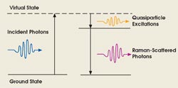
Figure 1. This energy level diagram shows the Stokes Raman scattering process involving a coupling between incident photons and quasiparticle excitations in a sample.
The frequency-downshifted (15.6 THz) Raman scattering, called Stokes scattering, is associated with optical phonons in silicon. The corresponding stimulated Raman scattering gain coefficient was shown to be more than 10,000 times larger in silicon than in glass (silica) optical fiber. Such a large nonlinear effect could make it possible to produce compact (centimeter size) active devices that are ideal for integrated photonic circuits in silicon.
Silicon waveguides
An optical waveguide is a fundamental element in integrated photonic circuits. Silicon waveguides usually are fabricated from silicon on insulator using standard CMOS techniques such as lithographic patterning and silicon etching (Figure 2). For optical amplification and lasing in silicon waveguides, it is essential that the waveguide transmission loss be as low as possible.
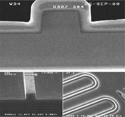
Figure 2. These are scanning electron microscope images of silicon photonic devices fabricated using standard CMOS technology. The top figure shows a silicon rib waveguide with oxide cladding. The lower left figure is a silicon rib waveguide without oxide cladding. The lower right figure shows 180° bent silicon waveguides.
To obtain a low-loss silicon waveguide, the waveguide sidewall roughness resulting from the fabrication process must be reduced because the refractive index contrast of the silicon waveguide system (Si/SiO2) is large (~2) and the roughness can contribute significantly to transmission loss when the waveguide dimensions are small. Although it is not yet possible to obtain optical transmission losses as low as in glass fiber (typically 0.2 dB/km), using state-of-the-art fabrication techniques, Intel achieves loss as low as 0.2 to 0.4 dB/cm for a waveguide size of ~1.5 × 1.5 μm. The small waveguide dimension reduces the pump power required for high Raman gain because the Raman scattering intensity is dependent on the pump intensity.
At the optical communication wavelengths of 1.3 to 1.6 μm, silicon is transparent for low power density light because the one-photon energy is smaller than the bandgap of silicon (1.17 eV). Under high optical powers, however, silicon becomes opaque because of the nonlinear optical loss associated with two-photon absorption as the combined energy of the photons exceeds the energy bandgap of silicon. Although the two-photon absorption around 1.55 μm is relatively small in silicon compared with III-V compounds, the induced free carriers can introduce significant optical absorption, which is proportional to the free carrier density.
In CW pumping, the induced free carrier density (Neff) is primarily determined by the competition between the carrier generation rate resulting from the two-photon absorption and the carrier decay rate and is given by
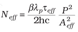
where β is the two-photon absorption coefficient, λp is the pump wavelength, h is the Planck constant, c is the velocity of light in vacuum, teff is the effective carrier lifetime that describes the carrier decay rate, P is the pump power and Aeff is the effective core area of the waveguide. Under normal circumstances, silicon has a relatively long (microseconds to nanoseconds) carrier recombination lifetime. It turns out that the free carrier absorption induced by two-photon absorption can exceed the optical gain through the stimulated Raman scattering and thus prevent achieving net gain in silicon.
To reduce the nonlinear optical loss of a silicon waveguide, one must reduce the free carrier density generated by two-photon absorption or shorten the effective carrier lifetime. There are several ways in which one can reduce carrier lifetimes in silicon, including by introducing defects in silicon. However, such an approach may induce additional loss in the waveguide.
In recent work, Intel researchers used a s ilicon waveguide that contains a PIN diode to reduce free carrier absorption. The PIN diode waveguide is constructed by ion-implanting a P-type region with boron and an N-type region with phosphorous in an intrinsic silicon slab (Figure 3). The P- and N-doped regions are far enough apart so that no light absorption from the doped areas occurs.
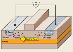
Figure 3. This schematic of a PIN diode silicon waveguide with reverse bias shows that the optical mode is confined in the intrinsic region between the P- and N-doped areas, and generates electron-hole pairs resulting from the two-photon absorption process. Under the applied electric field, the electrons move quickly to the N-doped region, while the holes move to the P-doped region.
When a reverse bias voltage is applied to the device, the external field accelerates the motion of photo-generated electrons and holes inside the waveguide so that they can be quickly swept out from the path of the light. As a result, the effective carrier lifetime (here, the carrier transit time) decreases. This leads to a decrease in the free carrier density and, in turn, reduction in the nonlinear optical absorption.
With this design, the researchers fabricated a low-loss PIN diode waveguide with a linear transmission loss of ~0.4 dB/cm for a waveguide dimension of ~1.5 × 1.5 μm, measured with a weak (<2 mW) incident light and no bias voltage applied to the diode. When the optical power inside the waveguide is high (e.g., 1 W) and the PIN diode is not biased, the waveguide transmission loss increases to ~1.6 dB/cm because of the free carrier absorption induced by two-photon absorption. However, the waveguide loss decreases to ~0.7 dB/cm when a reverse bias of 25 V is applied to the diode with the same optical power inside the waveguide.3,4
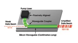
Figure 4. In this schematic of a silicon optical amplifier on a silicon substrate, a weak signal beam (red) is amplified by a strong pump beam (green) through stimulated Raman scattering.
As long as the nonlinear loss associated with free-carrier absorption in the silicon waveguide is successfully suppressed, silicon can amplify light. An example of a silicon optical amplifier based on the Raman effect is shown in Figure 4. In operation, two beams are coupled into the silicon waveguide. One is a strong optical pump beam with a wavelength of λp (in units of microns), and the other is a weak signal beam with a wavelength of λs. When the signal wavelength is tuned to the Stokes wavelength, given by
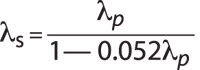
the weak signal experiences a maximum amplification from stimulated Raman scattering; namely, some of the pump energy converts into the signal beam.
To demonstrate the CW light amplification, the researchers performed a pump-probe experiment. Using a 4.8-cm-long waveguide containing a PIN diode with a reverse bias of 25 V, they demonstrated ~4 dB net CW gain with pump power of ~900 mW inside the waveguide. Because the Raman process is ultrafast, the silicon optical amplifier can amplify optical beams carrying high-bit-rate data. The researchers have amplified the light encoded with 10-Gb/s data without any signal distortion.
Optical amplifiers such as this are most commonly used to strengthen signals that have become weak after traveling a great distance. Because silicon Raman amplifiers are so compact, they could be integrated directly alongside other silicon photonic components, with a pump laser attached directly to silicon through passive alignment (Figure 4).
And because most optical devices, such as modulators, introduce transmission losses, an integrated amplifier could compensate for them, leading to lossless silicon photonic devices. In fact, the Intel researchers recently demonstrated a lossless optical modulator using a PIN diode silicon waveguide.5 Such a modulator is based on the fact that the stimulated Raman scattering gain is dependent on the reverse bias applied to the diode.
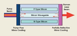
Figure 5. When a strong CW pump beam is coupled into the silicon waveguide cavity, stimulated Raman scattering amplifies the Stokes light as it bounces between two mirrors coated on the waveguide ends. As a result, a CW laser beam at the Stokes wavelength exits the silicon chip.
To create a laser, optical feedback must be added to the optical amplifier. The researchers coated the ends of the PIN diode waveguide with multilayer films to form an optical cavity (Figure 5). The multilayer coating is designed to have high reflection (low cavity loss) at the Stokes wavelength but low reflection at the pump wavelength for the input facet. This ensures that pump beam is efficiently coupled into the cavity. After applying a reverse bias voltage to the PIN diode waveguide and coupling a CW pump beam into the silicon waveguide cavity, the researchers observed a steady beam of light with a different wavelength exiting the cavity — the first CW silicon laser.6
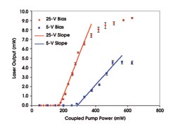
Figure 6. The laser output shows a strong dependence on the reverse bias applied to the PIN junction. The pump wavelength is 1.55 μm, and the Stokes wavelength is 1.686 μm.
Figure 6 shows the measured laser output power as a function of the input pump power for a 4.8-cm-long silicon waveguide cavity with an effective core area of ~1.7 μm2. The threshold and the laser slope efficiency depend on the bias voltage because the net gain inside the cavity is dependent on the bias voltage. With a reverse bias voltage of 25 V, the threshold power was ~180 mW and the slope efficiency was >4%.
The CW Raman silicon laser is single mode; that is, there is only one dominant oscillating longitudinal mode (side mode suppression is >55 dB), although several Fabry-Perot modes are within the Raman gain spectrum. The laser output spectrum linewidth was measured at <80 MHz and centered at the Stokes wavelength.
We note that Intel’s first CW Raman silicon laser was not optimized and that more work is needed. To decrease the lasing threshold, one could use even smaller waveguide dimensions (and, in turn, a smaller effective core area) and/or cavity enhancement of the pump power. One could also improve the PIN diode waveguide design to further reduce the effective carrier lifetime and possibly lower the reverse bias voltage.
The lasing slope efficiency can be optimized with the optical cavity length and with the cavity mirror designs. A waveguide-based ring cavity or Bragg grating reflectors could also replace the multilayer coating mirrors for possible monolithic integration.
Meet the author
Ansheng Liu is with Intel Corp.’s Photonics Technology Lab in Santa Clara, Calif.; e-mail: [email protected].
References
1. J.P. Russell (June 1, 1965). Raman scattering in silicon. APPL. PHYS. LETT, pp. 223-224.
2. J.M. Ralston and R.K. Chang (September 1970). Spontaneous-Raman-scattering efficiency and stimulated scattering in silicon. PHYS. REV. B., pp. 1858-1862.
3. R. Jones et al (Jan. 24, 2005). Net continuous wave optical gain in a low loss silicon-on-insulator waveguide by stimulated Raman scattering. OPT. EXPRESS, pp. 519-525.
4. H. Rong et al (Jan. 20, 2005). An all-silicon Raman laser. NATURE. pp. 292-294.
5. R. Jones et al (March 7, 2005). Lossless optical modulation in a silicon waveguide using stimulated Raman scattering. OPT. EXPRESS, pp. 1716-1723.
6. H. Rong et al (Feb. 17, 2005). A continuous-wave Raman silicon laser. NATURE, pp. 725-728.