Silicon photonics initially emerged to boost the efficiency, scalability, speed, flexibility, and connective capacity of massive data centers. Today, leading photonic transceiver players each report annual run rates of up to 2 million devices. And yet, even as the coronavirus pandemic has caused chaos and uncertainty around the world, the pace of innovation for these devices has accelerated, with new applications sprouting like wildflowers after a rain. Applications for silicon photonics include:
• Chip-based lidar, which gives sight to autonomous vehicles.
• Quantum computing, in which even the most nonphotonic qubit implementations require electromagnetically quiet and thermally adiabatic photonic interconnects.
• Photonic computing, which offers inherent strengths for artificial intelligence and inference applications.
• Photonic sensors, which are poised to revolutionize medical sensing via consumer wearables.
• Photonic cables, which offer throughputs that match the advanced buses
inside today’s computers but over lengths spanning many meters.
In short, silicon photonics has become a platform for a diverse set of applications, and it could well be the most consequential and disruptive advancement in semiconductors since the integrated circuit.
And therein lies the problem.
The tremendous breadth and the exploding volume of these new applications will escalate annual demand for silicon photonics devices by three orders of magnitude compared to the consumption by today’s data center-centric market. This puts pressure on manufacturers to rapidly ramp up production within the next five years.
The problem with success
Silicon photonics is an umbrella term that refers to the manufacture of photonic devices and circuits on wafers using proven semiconductor-fabrication processes and equipment. This allows the minting of thousands of photonic integrated circuits (PICs) per wafer, to produce sophisticated, multichannel devices with functionality, capacity, efficiency, and robustness that are beyond the scope of assemblies based on classical optics. Microelectronic and MEMS structures can be integrated alongside photonic elements, further boosting the capabilities of these miniaturized devices. And alternative planar substrates and materials allow for the integration of active optical elements such as detectors and lasers based on gallium arsenide or indium phosphide compounds, as well as highly selective silica-based arrayed-waveguide gratings. Polymer-based technologies are also advancing for on-chip elements, interconnects, and large substrates.
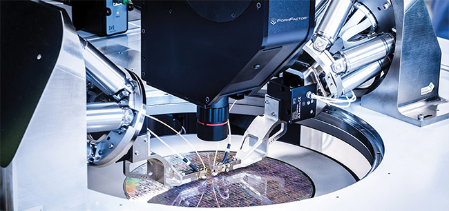
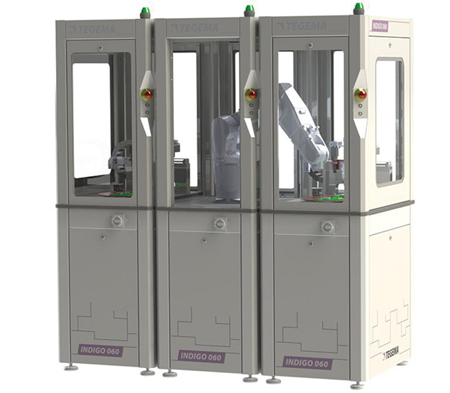
Automated solutions, such as FormFactor’s wafer prober (top) and Etteplan’s modular photonic assembly platform (bottom), will help to ramp up production of silicon photonics devices to meet burgeoning demand. Courtesy of FormFactor Inc.
The unfolding opportunities for silicon photonics are cause for excitement, and they have attracted considerable investment. A more worrisome consideration is the large ramp-up in volume of silicon devices that the new applications listed above will require. Projections indicate that hundreds of millions of devices will need to be produced to fulfill the demand for each of them.
Importantly, silicon photonics can be produced using established CMOS manufacturing tooling, but differences in production techniques begin at the very start of the manufacturing process.
First, the physics of photonics dictates larger structures than those seen in advanced microlithographic nodes, meaning that the exquisite recent-generation tools that keep pace with Moore’s law are overkill for silicon photonics.
Additionally, testing chips on-wafer — an essential step toward ensuring sustainable production economics — requires photonics-enabled probing tools that are capable of multiple degrees of freedom and high-speed nanoscale alignment. Similar capabilities are also needed for subsequent steps in downstream assembly, as well as throughout the packaging process.
Further, achieving such a leap in production requires synchronous global development on several fronts, including automation innovation that can lower costs of broadscale production, improved access to resources via public-private partnerships that span Europe and the U.S., and the implementation of scalable capacity in regions of high expertise.
Automation, partnerships, and pilot lines
The photonics industry today resembles the semiconductor industry of the mid-
1980s, when the rich ecosystem of semiconductor tool manufacturers was just emerging. Most processes remained labor-intensive and used custom-integrated tools.
Today’s photonics sector is in similar straits. Test toolmakers such as prober player MPI and photonics engineering prober pioneer FormFactor have only just emerged, along with microassembly powerhouses Etteplan (formerly Tegema) and ficonTEC. Many custom tools, however, continue to be built by dedicated integrators, much like in the semiconductor industry in its early days.
A recurring issue is the nanoscale alignment requirement mentioned above. It is the biggest manufacturing cost in PIC manufacturing. Fortunately, easily integrated, fab-class, autonomous microrobots and stage stacks are now available that can automatically optimize all the inputs, outputs, and degrees of freedom presented by these devices in one quick step. This reduces the time to align array devices with their multiple channels to less than a second, dovetailing neatly with the productivity targets that the industry is demanding.
The photonics industry
faces a gut check as its
past success drives future
demand at a scale and pace
that the industry will be
challenged to meet.
Many regions have promoted public-private partnerships to bootstrap regional production capabilities and now offer resources for the global photonics industry. China, for example, has made the advancement of photonics a broad national focus, while initiatives such as AIM Photonics in the U.S. are applying the unified approach on a smaller though still effective scale. In 2009, the European Union (EU) designated photonics as a key enabling technology for its role in building an autonomous European economy. The EU’s intent was to avoid repeating the mistakes of the 1990s, when low-cost labor in Asia bled the semiconductor and electronics industries out of the Continent.
The cascading impact of these losses collapsed the
EU’s value chain, from R&D to design, materials, components, logistics, and, most importantly, its exports of semiconductor and electronic devices. If unaddressed, China’s massive investments in photonics would mean it would only be a matter of time before it again overtook Europe in R&D and innovation for a vital sector.
The EU’s designation of photonics as a key enabling technology in 2009 led to the commitment of €120 million ($132 million) over the subsequent seven years. The goals of the investment were to
fund public-private initiatives aimed at lowering commercial and technological barriers to innovation, and to enable
European enterprises to scale up manufacturing of key photonics technologies. Further investment has since followed, yielding the EU’s thriving network of platform- and process-developing enterprises. These include projects ranging from the library-focused PLAT4M to the life sciences-focused PIX4life, as well
as ACTPHAST4.0, PIXAPP, JePPIX, PHIX, CITC, and the newest entrant, packaging-process-focused PODIUM,
a Dutch photonics consortium funded
by PhotonDelta.
Contract manufacturers
Contract manufacturers, which build products on demand for clients who are more focused on product development, are a familiar if underappreciated aspect of the silicon photonics sector. The assembly capabilities of some contract manufacturers — as well as a subset of outsourced semiconductor assembly and test enterprises — can be utilized during
the development of silicon photonic proto-
types when volumes are low, and then scale to meet growing demand. Top-tier silicon photonics players
have utilized partners like these for nearly a decade to help them deliver millions of products. Examples of companies that are utilizing such partners are Integra Technologies — a fast-turnaround Silicon
Valley fixture that offers capabilities across a wide range of chip test and packaging processes — and Benchmark Electronics, which offers packaging,
termination, and hybrid module assembly.
Combining resources
The photonics industry faces a gut check as its past success drives future demand
at a scale and pace that the industry will be challenged to meet. Its marquee
application — data center connectivity
— will soon be eclipsed by half a dozen other applications characterized by staggeringly higher projected volumes. To successfully confront this challenge, silicon photonics manufacturers must bring multiple capabilities and resources together. Fortunately, these capabilities and resources need not be created from scratch. They already exist: Fast, parallel alignment automation addresses the costliest aspect of the PIC manufacturing process. Public-private collaborations document best practices and provide
scalability expertise. And collaborations with contract manufacturers can quickly help companies to scale up production
to keep pace with exploding demand.
Leveraging these resources will be essential as the silicon photonics industry ramps up to meet its future.