The future of computing may need a light touch – literally. As chips move more and more data around, the metallic wiring on and between them eventually won’t be able to keep up.
The solution may be silicon photonics, a technology that employs silicon as an optical material. If compatible with standard CMOS semiconductor processing, silicon photonics promises inexpensive optical devices, easy integration with electronics and speedy data delivery.
First, though, researchers must grapple with a variety of issues, including reducing the cost to virtually nothing and finding ways to overcome a basic material drawback.
“The fundamental problem is silicon doesn’t emit light. It’s an indirect bandgap material,” said John Bowers, a leading researcher in the field and a professor of electrical and computer engineering at the University of California, Santa Barbara.
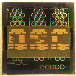
Optical buffers built in silicon, such as this chip, could be used as building blocks for silicon photonic circuits. The rings seen here function as long delay lines. Courtesy of John Bowers, University of California, Santa Barbara.
Researchers are working to solve this problem by incorporating more emission-efficient III-V semiconductor compounds such as indium phosphide or indium gallium arsenide. Another possibility would be to produce the light off-chip and use silicon only for modulation, routing and detection.
With regard to the latter, silicon photonics can outperform existing approaches. For example, Bowers and others demonstrated a silicon-germanium avalanche photodiode with better performance than one built with more conventional III-V semiconductors.
Companies are already putting silicon photonics to work. A look at near-term prospects – and some far-out ideas – shows where the technology is headed.
The five-meter solution
“We’re not trying to solve the 100-km problem, like in telecom. We’re trying to solve the five-meter problem,” said Mario Paniccia, photonics technology lab director at the biggest chipmaker of them all, Santa Clara, Calif.-based Intel Corp.
Doing so would allow servers to talk to each other over fiber and solve some data center bandwidth, thermal and cost problems. That’s because less power would be needed to move data, and having higher bandwidth could allow system architecture changes.
Being able to bridge 5 m with an inexpensive optical connection also would allow a single thin cable to connect devices in a home. Furthermore, notebooks could be thinner because connectors would be less bulky yet would offer higher bandwidth.
Intel recently announced its Light Peak optical interconnect technology, along with plans to ship product this year. On the photonics side, there’s an optical transceiver chip that moves data over distances of less than 50 m.
Multiple vendors will supply the optical chips, Paniccia said. The first-generation modules will consist of 850-nm vertical-cavity surface-emitting laser-based technology. They will offer two independent channels at 10 Gb/s. In the future, the technology will boost the rate to 100 Gb/s.
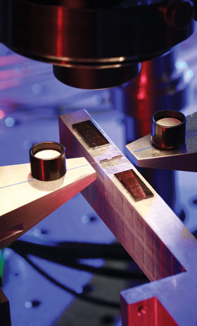
Future computer communication likely will travel over fiber, using transceivers to translate from photons to electrons and back. Here, a 40-Gb/s optical modulator is being tested. Courtesy of Intel Corp.
Another silicon photonics approach comes from privately held Luxtera Inc. of Carlsbad, Calif. The company’s philosophy, said vice president of marketing Marek Tlalka, is to route photons on a CMOS chip, much as is done with electrons, and to do everything in a mainstream CMOS manufacturing process.
Because silicon absorbs light in the visible and near-infrared ranges, those guidelines have implications for photonics, Tlalka said. “To transmit light on a CMOS chip, you need to operate at a longer wavelength, in the range of 1300 to just sub-1600 nm.”
Luxtera has chosen to use 1490-nm lasers, which are surface-coupled into waveguides. These waveguides, in turn, send the light into silicon modulators that can toggle the beam on and off 10 billion times per second. Multiple modulators, arranged in parallel or multiplexing at different wavelengths, will allow scaling of data rates to the 100-Gb and, ultimately, the terabit ranges.
The technology today, the company claims, allows 10-Gb connections at a cost per port in volume of less than $50, one-tenth that of other optical technologies and comparable to the electrical equivalent. However, their silicon photonics technique uses less than one-third the power of an electrical approach.
Luxtera spent years perfecting its manufacturing recipe, working with partners on such things as the best way to deposit and then etch germanium, which is required for integrated photodetectors. In selling its products, the company faced a problem. Most data center optical connections are done using 850-nm light, a wavelength incompatible with Luxtera’s technology. The company resolved this issue by making its first product what it called an active optical cable, which allows the longer wavelength to be employed without affecting users.
Farther out and closer in
Data transmission challenges also are expected to crop up for chip-to-chip and even subchip distances. Microprocessors, which today may have two or four cores, eventually will have hundreds of cores, all running independently while swapping data back and forth. Estimates are that today 40 percent of the power needed to run a chip is consumed by moving data on and off the device. Higher data rates and more cores will drive this number higher, unless something is done.
Ray Beausoleil, a physicist at Hewlett-Packard’s research labs in Palo Alto, Calif., noted that photonics can solve this problem. “Using light allows you to spend much less energy to send a signal from a transmitter to a receiver. It also allows you to significantly increase the number of connections that you have by using wavelength division multiplexing.”
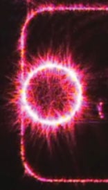
Shown here is a U-shape waveguide that glows because the light is tuned to the resonant frequency of the ring in the center. In practice, this structure would act as a modulator by injecting charge into the silicon, thereby tuning the ring’s frequency as needed to allow light to pass, or to stop it from doing so. Courtesy of Hewlett-Packard.
The work by Beausoleil and others at HP Labs is aimed at driving down the cost in dollars and the energy of computer interconnects. On the money side, the connections have to be essentially free. As for the energy expense, that too has to be almost nothing. The goal is to get as close as possible to 100 fJ per bit transmitted, roughly 10 times better than the current best research results.
Beausoleil, Bowers and others recently published a paper on a compact hybrid silicon microring resonator laser, the type of device that could act as an on-chip light source. It’s a hybrid because it uses a III-V semiconductor material, along with silicon, to generate continuous-wave laser light in a structure with a 12.5-µm radius.

A hybrid silicon ring laser, like the three shown here, could be used as an on-chip light source in future photonic circuits. The 12.5-µm-radius rings in the image consist of a III-V compound semiconductor. Waveguides – the black lines running below the rings – connect two integrated photodetectors. Courtesy of Di Liang, University of California, Santa Barbara.
Beausoleil noted a number of challenges in chip-scale silicon photonics. Still to be decided are fundamental questions such as whether to put the light source on the chip or to bring it in. He added, though, that the new technology may be able to piggyback on trends in the electronics industry.
Currently, chips are two-dimensional, but interconnect needs are forcing the industry into the third dimension. In the future, chips essentially will be stacked atop one another. As a result, memory and logic functions may be on separate layers. A photonic networking layer could be implemented on top of that, allowing on-chip optical routing.
That’s a solution being investigated by Yurii Vlasov, manager of silicon integrated nanophotonics at IBM in Yorktown Heights, N.Y. He noted that implementing such a layer creates numerous hurdles. For example, a running chip generates heat, causing a temperature rise of as much as 30 °C. That rise isn’t uniform or stable, Vlasov said. Instead, there are hot spots, which move around as circuitry switches on and off.
Designing optical components to handle such heat swings will be a challenge, especially given that the devices must be compact, inexpensive, low in power usage and CMOS-compatible. Nonetheless, suitable switches, modulators, wavelength division multiplexing filters and detectors have been demonstrated, at least in a laboratory.
Although Vlasov doesn’t expect on-chip silicon photonics to appear soon, the day also isn’t that far off, he said. “We have all the building blocks. It is now a question of putting it all together.”