To overcome the challenges of single-mode lasing with a high Q factor, researchers from Shanghai Institute of Optics and Fine Mechanics and collaborators demonstrated a single-frequency ultranarrow linewidth erbium-doped lithium niobate (LN) microdisk laser. The team achieved this through simultaneous excitation of high-Q polygon modes at both pump and laser wavelengths.
To enable applications ranging from lidar to metrology, on-chip microlasers must be operational at ultranarrow linewidths and high wavelength tunability. A high Q factor is used to achieve this.
According to the Schawlow-Townes theory, increasing the Q factor will lead to quadratic reduction of a microlaser linewidth. The highest Q factors to date have been those of whispering-gallery mode (WGM) microcavities in which light confinement is achieved through the continuous total internal reflection around the smooth circular periphery.
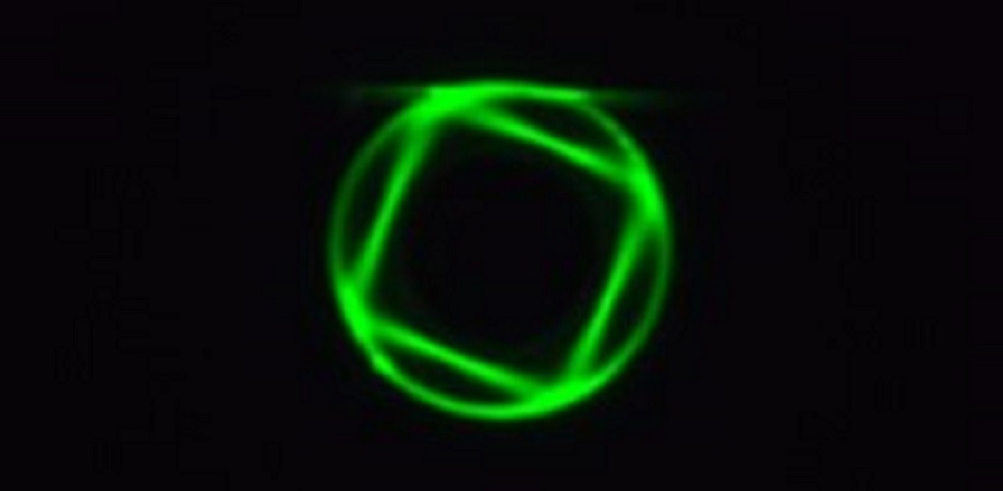
Coherent combined polygon mode for ultranarrow-linewidth, single-frequency microdisk laser. Courtesy of Jintian Lin/Shanghai Institute of Optics and Fine Mechanics.
However, the dense WGMs within the optical gain bandwidth typically give rise to multimode lasing in the microcavity. In principle, single-mode lasing can be achieved by reducing the size of the WGM microcavity, owed to the broadening of the free spectral range (FSR). However this strategy inevitably leads to increased radiation loss, which is detrimental to laser generation.
The erbium-doped LN microdisk was developed using photolithography-assisted chemomechanical etching (PLACE) to fabricate the LN microcavities integrated with microelectrodes in a controllable and cost-effective way. The microcavities provided an ultrasmooth surface, which enabled ultrahigh Q factors for the cavity WGMs.
The polygon modes were coherently combined by multiple WGMs triggered by a weak perturbation from a tapered fiber. The polygon modes were sparse within the optical gain bandwidth compared to the WGM counterpart, while their Q factors remained ultrahigh, which resulted in single-frequency lasing with a linewidth as narrow as 322 Hz.
Additionally, the system offered real-time electro-optical tuning of the microlaser wavelength, thanks to the strong linear electro-optic coefficient of LN.
The researchers’ method and outcome hold significant implications for miniaturized optical systems, which must incorporate highly coherent laser sources. Further exploration of the strong piezoelectric, acousto-optic, and second-order nonlinear properties of the LN substrate promises to advance the performance and functionality of the single-mode microdisk laser, to bypass the need for heterogeneous integrations.
The research was published in Advanced Photonics (www.doi.org/10.1117/1.AP.4.3.036001).