As the performance capabilities and sophistication of these detectors have expanded, so too have their value and impact in applications ranging from astronomy to the life sciences.
MICHEL ANTOLOVIC, PI IMAGING TECHNOLOGY, AND RAINER ERDMANN, PICOQUANT GMBH
As their name implies, single-photon avalanche diodes (SPADs) detect single particles of light, and they do so with picosecond precision. Single-pixel SPADs have found wide use in astronomy, flow cytometry, fluorescence lifetime imaging microscopy (FLIM), particle sizing, quantum computing, quantum key distribution, and single-
molecule detection. Over the last 10 years, however, SPAD technology has evolved through the use of standard complementary metal-oxide-semiconductor (CMOS) technology. This paved the way for arrays and image sensor architectures that could increase the number of SPAD pixels in a compact and scalable way.
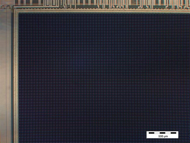
A 512 × 512 single-photon avalanche diode (SPAD) image sensor (top) and a closer look at the surface of the same (bottom). Courtesy of Pi Imaging Technology.
Compared to single-pixel SPADs, arrays offer improved spatial resolution and signal-to-noise ratio (SNR). In confocal microscopy applications, for example, each pixel in an array acts as a virtual small pinhole with good lateral and axial resolution, while multiple pixels collect the signal of a virtual large pinhole.
However, early SPAD arrays manufactured using CMOS technology exhibited low sensitivity and high noise. Since each SPAD required a protective guard ring and pixel-integrated electronics, arrays based on these detectors also suffered from low fill factors.
More recently, tailored fabrication processes, design improvements, and the use of optimized micro-optics have enabled current SPAD arrays to overcome these limitations and reach sensitivities and noise levels comparable to single-pixel devices.
SPAD arrays and image sensors are thus emerging to revolutionize confocal microscopy, as well as other fields that require improved spatial and temporal resolution from the photon-counting detectors applied.
Why use SPADs?
While conventional photodetectors,
photodiodes, and many avalanche photodiodes may offer higher sensitivity as quantified by quantum efficiency, SPADs excel at reading low-light signals, as quantified by their high SNR (Figures 1 and 2).
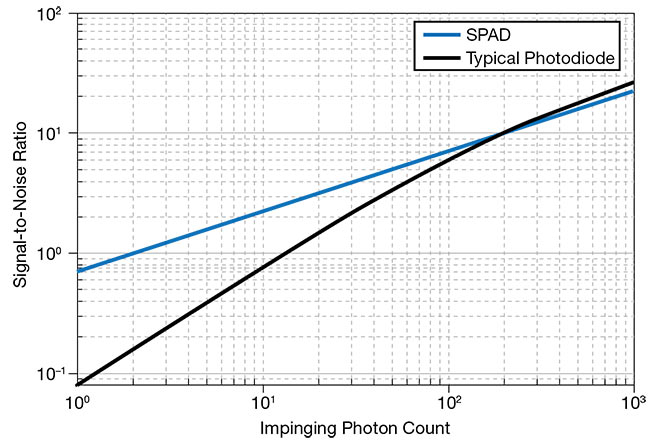
Figure 1. A signal-to-noise ratio (SNR)
comparison between a SPAD with 50%
sensitivity and a typical photodiode with 80% sensitivity, both with equivalent readout noise of 10 e− (representative only for high-speed readout mode). Courtesy of Pi Imaging Technology.
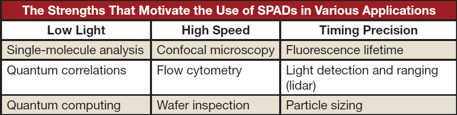
Low-light signals typically arise from faint light emitters such as small particles, low transmission, or fast imaging speeds. In addition to exhibiting high SNR when detecting low-light signals, SPADs are particularly precise (<150 ps) at measuring the timing of events. This is a direct consequence of their strong charge multiplication gain. These characteristics of SPADs make them appealing detectors in the applications summarized in the table above.
Early SPADs produced as single-point detectors in custom processes offered poor scalability. In 2003, researchers started using standard CMOS technology to build SPAD arrays. This change in design and production platform opened up the possibility to reliably produce high-pixel-count SPAD detectors, as well as invent and integrate new pixel circuity for quenching and recharging, time tagging, and photon-counting functions. Data handling in these devices ranged from simple SPAD pulse outputting to full digital signal processing.


Figure 2. A demonstration of SNR differences between a typical photodiode with 80% sensitivity and 10 e− signal (representative only for high-speed readout mode) equivalent readout noise (top) and a SPAD with 50% sensitivity (bottom), both at 10 impinging photons average. Courtesy of Pi Imaging Technology.
Over the subsequent decade, SPAD arrays primarily attracted research funding to make use of their excellent timing precision. This led to a plethora of array architectures and end-use cases. Among the most prominent applications resulting from this trend was the use of SPAD arrays in lidar, though the technology was also adopted in volume for integration into smartphones, where SPADs serve as proximity sensors capable of switching functionalities from idle to operational mode.
Research on SPADs also focused on the technology’s potential in biomedical applications, such as Raman spectroscopy, FLIM, and positron emission tomography (PET). Researchers in these fields have proposed very advanced architectures that aim to improve Raman detection by time gating, to leverage pixel parallelization to avoid the pileup effect in FLIM, and to improve PET spatial resolution by exploiting SPAD timing resolution. However, SPAD technology’s lower sensitivity, higher noise, and longer innovation cycles inhibited its early adoption in these applications.
Advancements made within the past decade, however, have improved SPAD array sensitivity from the typical 30% peak sensitivity to more than 50% peak sensitivity and reduced dark noise from the typical 100 counts per second (cps)/µm2 to less than 1 cps/µm2.1,2
The challenges of CMOS SPADs
Many early CMOS SPAD designs used 0.35-µm fabrication processes in which standard layers were used to create the SPAD junctions. Consequently, performance of these junctions was nonoptimal when a high electric field (~0.5 MV/cm) was applied to enable the device to work in the avalanche mode. In most cases, surface and silicon impurities together with noncontrollable lateral electric fields also increased detector noise. Sensitivity was also not optimal because developers typically fabricated shallow layers with high doping to achieve high electric fields. The shallow junctions led to a lower detection efficiency with a typically blue-shifted sensitivity peak.
With the development of more advanced semiconductor processes, the SPAD array community started using 180-, 110-, 65-, and 40-nm process nodes to improve the functionality of its SPAD devices and build more advanced architectures. However, in many cases the higher doping, and sometimes shallower layers, applied in smaller semiconductor nodes also led to poorer SPAD performance.
Additionally, SPADs require a lateral protective guard ring measuring 1 to 2 µm in width and more electronics than conventional sensors. This further decreases sensitivity due to the lower geometrical fill factor, which at one point was well below 3%.
Substantially increasing the pixel resolution of SPADs was, and still is, challenging for three reasons. SPADs are larger than conventional pixels due to their prerequisite guard ring. They consume more power due to larger signal amplitudes versus conventional photodiodes. And they generate more data if used in event-timing modes.
Close collaboration between SPAD developers and CMOS fabs, however, has helped SPAD technology overcome many of its sensitivity and noise challenges by adding SPAD-specific layers into the semiconductor process flow, design innovations in SPAD guard rings, and enhanced fill factors made possible by microlenses.
The power requirements and data rate of SPADs were also reduced through the development of novel architectures based on photon selection occurring as close as possible to the SPAD pixel. Examples include the time-gating technique applied in SPAD image sensors, filtering of time-tagging events by time correlation, and inducing photon count compression through nonlinearity.
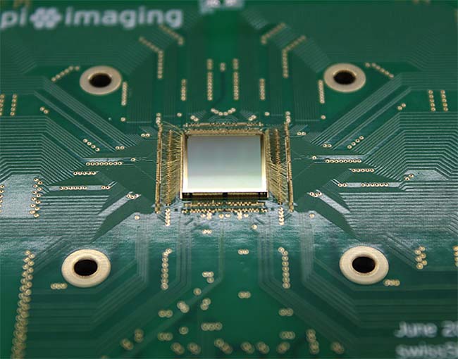
These synergistic effects finally led to the development of large SPAD image sensors that incorporated 512 × 512 and higher pixel counts (see image at beginning of article).
SPADs in application
Time-resolved confocal microscopy is a powerful tool that has become an established tool in life science research. It allows, for example, the quantification of molecular dynamics, the sensing of cellular environments, and the study of protein interactions. A confocal microscope offers excellent spatial resolution while minimizing phototoxicity through judicious control of excitation power. However, confocal microscopy suffers from a fundamental trade-off between signal intensity and resolution: A smaller pinhole ensures confocality, which improves resolution and sectioning performance, but at the cost of lower signal intensity.
When applied in image scanning
microscopy (ISM), SPAD arrays eliminate this trade-off and improve both the spatial resolution and signal intensity. ISM increases the spatial resolution of confocal microscopes by replacing the conventional single-point detector with
a pixel array to record multiple images from various angles. Each pixel of the SPAD acts as a virtual small pinhole
with good lateral and axial resolution, while multiple pixels collect the signal of a virtual large pinhole. The result is a final image with improved resolution obtained by applying a mathematical method called pixel reassignment (Figure 3).
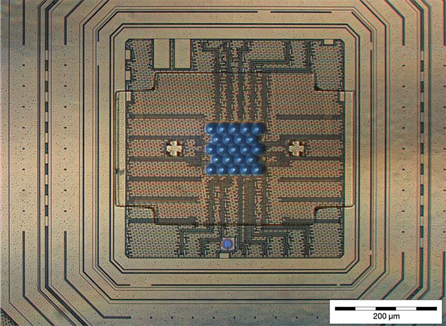
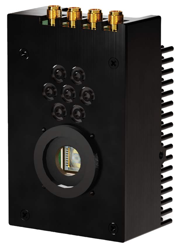
Figure 3. A compact SPAD microarray chip with 23 pixels (top), and a system implementation for image-scanning microscopy applications (bottom). Courtesy of Pi Imaging Technology.
FLIM is a powerful modality in confocal microscopy. It is often used for
dynamic live-cell imaging and for studying protein interaction via Förster resonance energy transfer (FLIM-FRET) (Figure 4). FLIM is also finding broader application in materials science, where it is used to study semiconductor properties or processes such as charge-carrier diffusion.
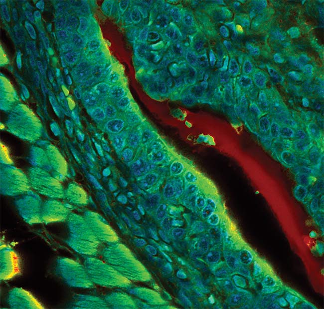
Figure 4. A fluorescence lifetime imaging microscopy (FLIM) image of mouse embryo tissue recorded with a single-photon-counting confocal microscope. Courtesy of PicoQuant.
Many substances — including organic fluorophores, fluorescent proteins, and nanoparticles (e.g., quantum dots and nanodiamonds) — emit photons after absorbing light in a process called fluorescence. Each emitting substance has a characteristic fluorescence lifetime that indicates how long it remains in an electronically excited state before returning
to the ground state.
FLIM produces an image based on the differences in excited-state decay rates, enabling an imaging technique where the contrast is based on the lifetimes of individual fluorophores rather than their emission spectra. A FLIM image consists of a 2D grid of pixels that divides the sample into small areas of identical size. For each pixel, the fluorescence lifetime is determined by means of time-correlated single-photon counting. This technique positions the microscope’s excitation laser at each segmented area of the sample to collect the arrival times of emission photons with a corresponding single-pixel detector such as a SPAD. The photon
arrival times for each pixel are sorted into a histogram from which the fluorescence lifetimes can be extracted via various mathematical methods.
FLIM benefits from the use of SPAD arrays, which allow faster imaging speeds by increasing the sustainable count rate via pixel parallelization. SPAD image sensors enhanced with time-gating functions can further
expand the implementation of FLIM to nonconfocal microscopic modalities and thus establish FLIM in a broader range of potential applications, such as spatial multiplexed applications in a variety of biological disciplines including genomics, proteomics, and other “-omics” fields.
One additional application where SPAD technology is forging performance enhancements is high-speed imaging, in which image sensors typically suffer from low SNR. The shorter integration times in these operations lead to lower photon collection and pixel blur, while the faster readout speeds increase noise in the collected image. SPAD image sensors fully eliminate this noise to offer Poisson-maximized SNR.
It’s about time
Due to the tremendous developments
in CMOS SPAD technology, more advanced SPAD arrays and image sensors
are emerging to revolutionize not only confocal microscopy but also other fields that require improved spatial and temporal resolution from photon-counting detectors.
SPAD arrays represent an exciting opportunity for confocal microscopes because they potentially improve all crucial performance parameters, including SNR, acquisition speed, the threshold for excitation intensities, and spatial and timing resolution — all with very little to no increase in system complexity.
In parallel, SPAD arrays are introducing new opportunities to expand FLIM solutions to imaging modalities used for drug development, medical diagnostics, and surgery assistance. Further, SPAD image sensors hold the potential to enrich the capabilities of high-end image sensors, similarly to how electron multiplying CCDs did in the past.
Meet the authors
Michel Antolovic is CEO of Pi Imaging Technology, a company developing and commercializing advanced SPAD arrays and image sensors in CMOS technology. He has an extensive background in semiconductor technology and photonics; email: [email protected].
Rainer Erdmann is the founder and managing director of PicoQuant GmbH, a developer and manufacturer of high-quality photonic components and time-resolved fluorescence
instruments targeting a broad range of scientific applications; email: [email protected].
References
1. I.M. Antolovic et al. (2018). Dynamic range extension for photon counting arrays.
Opt Express, Vol. 26, No. 17, pp. 22234-22248, www.doi.org/10.1364/oe.26.022234.
2. S. Mandai et al. (2012). A wide spectral range single-photon avalanche diode fabricated in an advanced 180 nm CMOS technology. Opt Express, Vol. 20, No. 6,
pp. 5849-5857, www.doi.org/10.1364/oe.20.005849.