Although the optical waveguides used in optical circuits allow much higher bandwidths than the fine copper wires that are used in electronic chips — and generate less heat — the size of optical integrated circuits is quickly reaching into the nanometer regime. This has necessitated discovery of new ways to drive and control their nanosize light sources efficiently.
In response to this need, researchers from Korea University have developed an all-optical method for driving multiple highly dense nanolaser arrays that could enable chip-based optical communication links that process and move data faster than current electronic devices. In the research, the use of optical fiber eliminated the need for large and complex electrodes that are typically used to drive laser arrays.
According to research team leader Myungi Kim, this enabled the researchers to reduce the overall dimensions of the laser array and also eliminate heat generation and processing time delays that come with electrode-based drivers.
The development of optical interconnects equipped with high-density nanolasers would improve information processing in data centers, including those that move information across the internet, Kim said. “This could allow streaming of ultrahigh-definition movies, enable larger-scale interactive online encounters and games, accelerate the expansion of the Internet of Things, and provide the fast connectivity needed for big data analytics,” he said. “Optical devices integrated onto a chip are a promising alternative to electronic integrated devices, which are struggling to keep up with today’s data processing demands.”
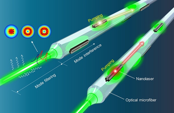
Researchers have developed an optical fiber-based method for driving multiple high-density nanolaser arrays using light traveling down a single fiber. The optical driver creates programmable patterns of light via interference. Courtesy of Myung-Ki Kim/Korea University.
The researchers used a unique optical driver that creates programmable patterns of light via interference as their alternative to the electrodes that are commonly used to pump nanolaser. This pump light travels through an optical microfiber onto which nanolasers are printed. To demonstrate this approach, the researchers used a high-resolution transfer-printing technique to fabricate multiple photonic crystal nanolasers spaced 18 µm apart. These arrays were applied onto the surface of a 2-µm-diameter optical microfiber.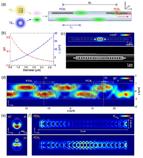
Simulation images show how the light interference pattern interacts with the nanolaser arrays. (a) Schematic of spatial interference between TE00 and TE01 modes along the microfiber. Here, two photonic crystal nanobeam lasers (PCN1 and PCN2) are attached to the surface of the microfiber in a line. (b) Difference in effective refractive index (Δn) of TE00 and TE01 modes and corresponding half beat length (Lπ). (c) Log |E|2 profile of PCN cavity mode in the xy-plane and SEM image of fabricated InGaAsP PCN laser. (d, e) |E|2 profiles of the pump beam in the xz- and yz-planes, respectively, where the beam propagates from left to right. (f) Absorbed power density profiles along the xy-plane at the vertical center of PCNs. Courtesy of Korea University.
This had to be done in a way that precisely aligned the nanolaser arrays with the interference pattern. The interference pattern could also be modified by adjusting the driving beam’s polarization and pulse width.
The experiments showed that the design allowed multiple nanolaser arrays to be driven using light traveling through a single fiber. The results matched well with numerical calculations and showed that the printed nanolaser arrays could be fully controlled by the pump beam interference patterns.
“Our all-optical laser driving and programming technology can also be applied to chip-based silicon photonics systems, which could play a key role in the development of chip-to-chip or on-chip optical interconnects,” Kim said. “However, it would be necessary to prove how independently the modes of a silicon waveguide can be controlled. If this can be done, it would be a huge leap forward in the advancement of on-chip optical interconnects and optical integrated circuits.”
The research was published in Optica (www.doi.org/10.1364/OPTICA.471715).