Size is everything when it comes to fabricating plasmonic structures.
For optical nanoantennas, for example, we’re talking about tens of nanometers
in length, with a gap of less than 10 nm. At this scale, even slight defects can
become a massive problem.
A new nanofabrication method developed by researchers at the University
of Würzburg could provide solutions for building high-definition complex plasmonic
nanodevices and extended optical nanocircuits.
One such device is the optical nano-antenna, which can collect
and concentrate light for more efficient photovoltaic power generation. But the
applications of nanoantennas do not stop there, researcher Bert Hecht said.
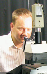
Bert Hecht examines an optical
nanoantenna developed using a new fabrication method developed at the University
of Würzburg. Courtesy of Bert Hecht.
“The ability to concentrate light is of interest in photovoltaics,”
he said. “The ability to concentrate light to subwavelength dimensions into
the nanometric antenna gap is of importance for optical sensors with single-molecule
sensitivity and for high-resolution microscopy. Furthermore, single molecules or
quantum dots coupled to antennas can lead to highly efficient single-photon emitters
for quantum communication.”
Today’s optical nanoantennas often are sculpted from multi-crystalline
evaporated thin films; more precisely, a thin layer of metal is applied to a carrier
substrate by means of vapor deposition. Then, just as in sculpting, desired patterns
can be worked into this “blank.”
The problem is that the base layer consists of many small individual
crystals, resulting in a grainy structure. When trying to cut smooth structures
with any kind of precision, the graininess can result in irregular shapes that can
render the device useless. This is mostly because various crystal facets etch with
different rates during the focused ion beam milling process.
Hecht’s team worked with researchers from Swiss Federal
Laboratories for Materials Testing and Research in Dübendorf, Switzerland,
and from Polytechnic University of Milan in Italy to come up with an alternative
way of preparing the gold substrate.
They used chemically synthesized gold flakes, which consist of
a single gold crystal, to avoid the problems caused by any internal granular structure.
By means of ion beam milling, they fabricated nano-structures from these flakes
that exhibit greater precision than ever.
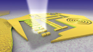
An artist’s rendition of a single-crystalline gold flake from which optical nanoantennas, among
other nanostructures, were fabricated with great precision. The optical nanoantennas,
which appear as cubes arranged in pairs, can collect and concentrate light 10 times
more efficiently than can multicrystalline antennas. Illustration by Thorsten Feichtner.
“We have found a simple method which allows everybody to
use single-crystalline gold to fabricate plasmonic structures of much higher quality
and much higher precision,” Hecht said. “This will allow us to realize
structures that were not possible before, and it will raise the overall quality
standards for plasmonic structures.”
The method is described in the Dec. 21, 2010, issue of Nature
Communications. In the approach, large and thin single-crystalline gold flakes are
chemically grown and deposited onto a glass/indium tin oxide surface.
From this more homogeneous structure, the group fabricated nanostructures
that exhibit ultrasmooth surfaces and small gaps over extended distances, not easily
achieved using other approaches.
“The use of single-crystalline gold allows us to produce
reproducible optical nanoantennas with very small tolerances,” Hecht said.
“Their optical properties – the light enhancement in the feedgap –
are roughly 10 times better than for multi-crystalline antennas.”
Although photovoltaic systems could stand to profit from easier
and cheaper ways to produce nanoantennas, Hecht admits that rooftop solar cells
probably will benefit from cheaper and simpler methods before nanoantennas become
sufficiently cheap and are able to be produced in large enough arrays.
Nevertheless, the investigators plan to follow up the potential
of antennas for optoelectronic applications.
“We will further push the limits of fabrication to produce
ultrasmall gaps, which should yield even higher field enhancement,” Hecht
said. “The reproducibility of the structures and their high precision are
instrumental for systematic studies of such effects. It will allow us to gain a
deeper understanding of the underlying physics.”