Compiled by Photonics Spectra staff
A simple technique for stamping patterns invisible to the human eye onto a special class of nanomaterials provides a new, cost-effective way to produce novel devices for a wide range of applications, including drug delivery, chemical and biological sensors, solar cells and battery electrodes.
The technique, developed by Vanderbilt University engineers, works with porous nanomaterials riddled with tiny voids that give them unique optical, electrical, chemical and mechanical properties. There are nanoporous forms of gold, silicon, aluminum and titanium oxide, among others.
Until recently, the processing that was required to transform these materials into devices was complex and expensive. Now, the researchers have developed a rapid, low-cost imprinting process that can stamp out a variety of nanodevices from the materials. They used a regular tabletop vise for their first successful imprint.
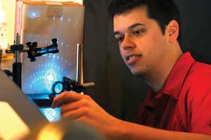
Vanderbilt graduate student Jason Ryckman demonstrates the operation of a new diffraction-based biosensor that is produced out of a nanoporous material by a new imprinting process. Courtesy of Anne Raynor, Vanderbilt University.
Traditionally, devices were made from nanoporous materials in a process similar to that used for computer chips: painting the surface with a resist, exposing it to ultraviolet light or scanning the surface with an electron beam to create the desired pattern, and then applying a series of chemical treatments to either engrave the surface or lay down new material. The more complex the design, the longer it would take to make.
Sharon M. Weiss, associate professor of electrical engineering, got the idea about two years ago to create premastered stamps using the complex process and then using the stamps to create the devices. The new approach, direct imprinting of porous substrates, can create a device in less than a minute, regardless of its complexity. The group reports that, so far, it has used master stamps more than 20 times without any signs of deterioration. Their smallest pattern has features of only a few tens of nanometers. In addition, they have succeeded in imprinting the smallest pattern yet reported in nanoporous gold, one with 70-nm features.
The first device the group made is a diffraction-based biosensor that can be configured to identify a variety of organic molecules, including DNA, proteins and viruses.
The group collaborated with colleagues in the chemical and biomolecular engineering departments to use the new technique to make nanopatterned chemical sensors 10 times more sensitive than another type of commercial chemical sensor called Klarite – the basis of a multimillion dollar market.
Details of the work appeared in the May 2011 issue of Nano Letters (doi: 10.1021/ nl1028073).