Barbara Stumpp, Science Writer
New calibration options enable significant improvements in the accuracy of new and old devices, which could mean big advances in materials for LEDs and lasers.
LEDs have numerous advantages over traditional light sources such as halogen or energy-saving lamps. They use electric power efficiently and, employed in combination with various-colored bodies, can be designed to provide an almost natural light. They are also completely jitter-free.
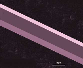
ZnO has shown potential as an active material for LEDs and solid-state lasers. Recent research has shown that the threshold for ZnO microwires as an active material for lasers is 73 kW/cm2 at room temperature. Here, ZnO microwires used during the tests at the University of Leipzig.
When today’s electronics light up, GaAs (gallium arsenide) and/or GaN (gallium nitride) are involved, which is not always a good thing. Gallium is rare – and priced accordingly – and the poisonous arsenic causes problems in disposal. GaN is a powerful but technologically difficult material to handle, resulting in a search for alternatives despite its high level of functionality. For research purposes and for industrial production of electronic lighting, LEDs and laser diodes, finding cheap and environmentally friendly alternatives is important.
Basic research has reset its focus on the semiconductor zinc oxide (ZnO), which has a direct bandgap comparable to GaAs and GaN, raising hope that one day blue LEDs will be made from this material. Moreover, ZnO is available in quantities suitable for industry and is inexpensive, nontoxic and simple to process. So far, however, one problem has prevented its use: It is impossible to generate high, homogeneous and stable p-type doping, which, at the moment, greatly reduces LED efficiency.
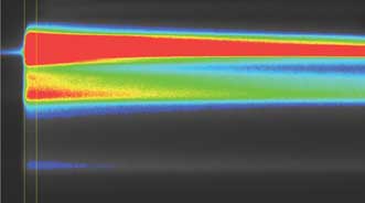
The decay of a laser-excited ZnO sample. The X-axis shows the time elapsed (0 to 2 ns), and Y-axis shows the spectral information.
ZnO also shows potential as an active material for solid-state lasers. Recent developments at the University of Leipzig Institute of Experimental Physics II, Semiconductor Physics Group, in Germany have shown that the threshold for ZnO microwires as an active material for lasers is 73 kW/cm2 at room temperature. But further research is needed to develop ZnO LEDs and lasers for industrial-scale applications, and streak cameras are helping in this endeavor.
Streak cameras are used for time-resolved analysis of ultrashort optical signals, and researchers at the University of Bochum in Germany are using them to make phenomena visible, examining – among other things – the time-resolved photoluminescence of ZnO.
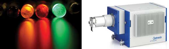
The OptoScope streak camera from Optronis GmbH enables research into the temporal behavior of the photoluminescence of ZnO at the University of Bochum.
These cameras achieve temporal resolutions in the range of picoseconds (10-10 to 10-12 s). Apart from their high temporal resolution, streak cameras are the only instruments that allow simultaneous measurement of the temporal behavior of multiple optical processes.
When measuring with a streak camera, the image of a slot is deflected at very high speed over a screen. If you know the deflection speed, you can connect the information received from the position on the screen with a time axis. The deflection is technically realized by a streak tube. Streak tubes are vacuum tubes that work – as with first-generation image amplifier tubes – with a photocathode to convert the light flux into a current of electrons, focusing electrodes and a phosphor screen to reconvert it into optical signals. A peculiar feature of the streak tube is that additional baffles allow a shifting of the image on the phosphor screen; a CCD camera then records the image.
The vertical profile – i.e., the spectral information of the sample’s decay – shortly after laser excitation.
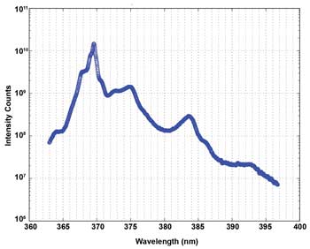
In combination with a spectrometer, the streak camera can perform time-resolved spectroscopy. The camera’s high sensitivity allows detection of even weak signals up to those of individual photons. Dr. Jan Heye Buß of Bochum University explores homoepitaxially grown zinc oxide using the OptoScope streak camera from Optronis GmbH of Kehl, Germany. The zinc oxide is activated by light of a wavelength of about 351 nm and an intensity of 10 to 12 mW. By visualizing the photon response, the research delves into the temporal behavior of the photoluminescence of this material.
The measurement errors of the Opto-Scope’s spot velocity and its linearity are specified to ±5 percent at maximum, but the delivered systems typically have presented an error of 2 to 3 percent. Depending upon the system configuration, additional errors can occur because of geometric image distortions and the specific transit-time distortion. Despite these errors, the camera system already has delivered good results for many measurement tasks without further corrections.
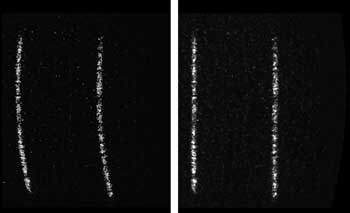
To make ZnO measurements, researchers sometimes work with very fast signals that can be detected only at high sweep rates, at which the photoelectron transit-time distortion of the streak tube becomes “visible” in the form of parabolic distortion; this can be corrected by the new software.
For materials research, the SC-10 streak camera from Optronis is used for measurements on ZnO, and the SC-20/SC-51 is generally used for detonics and laser Doppler interferometry.
“With the SC-20/SC-51, a correction of geometric image distortions (barrel, pincushion) is essentially helpful because the optical and electro-optical transmission components in respect to the streak camera have to transfer a large image,” said Dr. Patrick Summ, CEO of Optronis. “With the SC-10, this plays a minor role, as the image to be transferred is smaller by a factor of about 1.5 and, thus, the optical distortions are usually negligible.”
To make ZnO measurements, researchers sometimes work with very fast signals that can be detected only at high sweep rates. Here, the photoelectron transit-time distortion of the streak tube becomes “visible”: It makes itself noticeable therein, as parabolic distortion usually occurs from the center to the edge of the image. The reason for this is that the outer photoelectrons travel a longer distance in the tube. In this case, a correction of this transit-time distortion makes sense.
Streak cameras are used primarily in the field of basic research at universities and research institutes, and researchers need the best possible results because further research builds on these results; also, case-specific adjustments and the traceability of the determination of raw data are always relevant to research. To help researchers get the most from their results, the analysis software OptoAnalyse from Optronis offers simple and targeted calibration and correction functions.
The new software can enable correction of the transit-time distortion of the photoelectrons and the geometric image distortions as well as the absolute and relative calibration of the sweep rate.
An important issue in the implementation of these correction and calibration functions has been that the calibrations are done by a process that is easy to understand, Summ said. Transparent data processing leads to improved results. The user can thus decide in person which corrections are desirable, and the reference data can be directly accessed. The relevant measurements for the ZnO test results are thus available with an accuracy of 1 percent in range.
The development of future ZnO LEDs, new solid-state diode lasers and diode lasers, and ever-more-exclusive application areas would have been impossible – and cannot continue in the future – without basic research using streak cameras.
Meet the author
Dr. Barbara Stumpp is a freelance journalist in Freiburg, Germany; email: [email protected].