Superpolished crystalline substrates deliver important benefits for coated optics in demanding ultraviolet laser applications, but the successful use of the process requires a consideration of its unique subtleties.
David Collier and Rod Schuster, Alpine Research Optics
Demanding ultraviolet laser applications, such as microlithography and lasik, are driving the need for coated optics that deliver superior performance and longer lifetimes. Tremendous advances have been made in both areas in recent years, and to continue this progress, optical component manufacturers are turning to low surface roughness, or superpolished, substrates of UV-compatible crystalline materials such as CaF2 and MgF2.
Three primary loss mechanisms influence the performance of high-reflection thin-film coatings: transmission, absorption and scatter. Transmission and absorption can be addressed by refining design and fabrication. Both the coating and the surface roughness of the substrate can be limiting factors in minimizing scatter loss. Substrate roughness is particularly important because the overall roughness is maintained or even increased as a surface is coated with multiple layers of material.
Scattering causes several problems. The most obvious is loss of transmission, which might be as high as 2 percent per component for optics of average quality. For a system with multiple surfaces, loss can rapidly build to unacceptable levels.
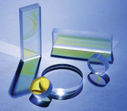
Figure 1. Manufacturers of deep-UV optics are using superpolished substrates to deliver coated components that provide higher performance and reliability and longer lifetimes.
Additionally, it has become accepted in the semiconductor microlithography industry over the past five to seven years that surface finish also affects the lifetime of coated beam-delivery optics. In part, this is because no substrate or coating material is completely nonabsorbing, particularly in the ultraviolet.
Although the absorption coefficient may be very low, scattering causes light to become “trapped”; that is, it is scattered from and trapped between multiple, rough layer interfaces, where some of it is eventually absorbed. Over time, this absorption causes damage, which leads to more absorption and, eventually, to thermal damage and to the failure of the substrate and/or of the coating. In the case of crystalline substrates, this damage can take the form of Schlieren or slipstream defects, in which local heating creates stress in the crystal lattice that is partially relieved by a slip between adjacent layers of atoms.
Just as important, surface finish also influences the mechanical adhesion of a coating. This affects the lifetime of the coating on the optic: The smoother the substrate surface, the better the coating adhesion and the longer the lifetime.
Surface roughness — and its effects on scatter loss and on component lifetime — becomes even more important at shorter wavelengths. For a given surface roughness, scatter increases strongly as wavelength decreases. Scatter intensity also scales nonlinearly with particle size. This means that surfaces used for 193-nm applications should be an order of magnitude (or more) smoother than surfaces used for visible applications to achieve the same scatter specification.
For these reasons, high-value and performance-critical optics in UV applications are increasingly incorporating superpolished surfaces. Typical commercial “laser grade” MgF2 and CaF2 optics are fabricated to have an Sq (rms surface roughness) of 10 to 15 Å. In contrast, superpolished deep-UV optics have an Sq of 1 to 2 Å.
Conceptually, superpolishing is a simple process, involving a sequence of successively finer grinding and polishing steps. At each step, the optics must be tested to ensure that they have reached the target roughness. However, a number of problems must be surmounted to consistently produce these ultrasmooth surfaces with CaF2 and MgF2 substrates, crystalline materials that are much softer than the fused silica used in longer-wavelength ultraviolet applications.
Although grinding and polishing are used to form the optical surfaces on all of these materials, the crystalline materials are worked by mechanical abrasion alone. In contrast, a conventional cerium oxide polish for silica works — at least, in part — by chemically removing material. Mechanically abrading the soft crystals can lead to subsurface damage, a phenomenon first identified by researchers at Lawrence Livermore National Laboratory in Livermore, Calif. Fractures and scratches that occur during the grinding and polishing process can become partially or totally covered by the polishing redeposition layer, a thin layer of material that flows while the material is being worked (Figure 2). Through this mechanism, residual polishing compound may become incorporated into the surface layer or deposited into microfractures and other surface defects.
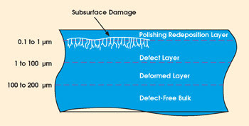
Figure 2. Subsurface damage causes fractures and scratches during the grinding and polishing process. Residual polishing compound may become incorporated into the surface layer or deposited into microfractures and other surface defects. To minimize their impact, polishing compounds should be highly transparent at the final operating wavelength and should be used to remove a layer of material twice the size of the grit used in the previous process step.
Superpolishing crystalline UV materials therefore demands that each finer process step completely remove the subsurface damage created by the previous step. As a rule, this involves the removal of a layer of material that is at least twice as thick as the previous grit size. For example, after grinding with 50-μm grit, the next step may be to use 20-μm grit to remove at least 100 μm of material. It also is important to employ grinding and polishing techniques that are designed to rapidly remove any debris that could cause surface scratches.
The nature of mechanical polishing and subsurface damage makes it inevitable that some microscopic amounts of polishing material will remain embedded in the surface after final processing. To minimize the impact of this effect, it is vital to use polishing compounds that are transparent at the operating wavelength of the final optical element.
One approach is to use a diamond-based abrasive mixed with deionized water. Diamond is highly transparent in the UV, including at the 157-nm excimer laser wavelength. To minimize contamination and scratching, the mixture is used only once, rather than being recirculated in a slurry as in conventional optics polishing. However, even diamond-based abrasives can contain impurities that absorb in the deep-UV. Vendors producing abrasive compounds thus should be qualified because not every supplier is capable of consistently delivering product with the necessary level of purity.
Finally, accurate testing is critical to successful superpolishing. A number of tools can measure roughness at the angstrom level —most notably, the atomic force microscope and the white-light interferometric microscope. The latter offers a good combination of real-time speed and rugged performance and thus is well-suited to in-process testing (Figure 3). The device’s speed is a direct consequence of its being an imaging device rather than a spot sampler or a transept profiler.
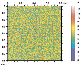
Figure 3. The white-light interferometric microscope combines real-time speed and rugged performance for measuring roughness at the angstrom level. Here, the instrument has produced a surface map of a superpolished CaF2 substrate, using false color to highlight surface roughness. The field of view of the instrument is 0.8 × 0.8 mm, and the rms surface roughness of the area is 1.48 Å.
Just as important, it is a true noncontact tool, unlike the atomic force microscope. To support the volume manufacturing of superpolished components, it is important that the instrument incorporate a software suite that provides surface relief images that can be rapidly interpreted as well as statistical information for archival purposes.
The superpolishing of crystalline substrates presents numerous production challenges but yields ultraviolet optics with superior characteristics. Although superpolished optics can be more costly than conventionally polished ones, their performance, reliability and lifetime can ultimately result in a lower total cost of ownership. For this reason, an increasing number of ultraviolet applications feature superpolished optics in the beam-delivery chain.
Meet the authors
David Collier is president and Rod Schuster is marketing manager at Alpine Research Optics in Boulder, Colo.; e-mail: [email protected].
Substrate Issues
Besides tightly controlling the substrate preparation and coating processes, achieving high performance and long lifetimes from superpolished deep-ultraviolet optics requires starting with high-quality raw material blanks that are free of impurities and defects.
Saint-Gobain Crystals & Detectors (formerly Bicron) of Solon, Ohio, is one of several suppliers of superior-grade CaF2 and MgF2 blanks. Jim DiCillo, optics manufacturing manager, explained that there are three factors to consider when supplying synthetic crystalline blanks for the production of superpolished optics.
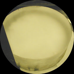
To successfully and consistently fabricate superpolished optics, blanks are cut from boules of raw CaF2 crystal that are free from impurities and defects. Courtesy of Saint-Gobain Crystals & Detectors.
The first involves the material quality of the blanks. Saint-Gobain uses ultrapure raw materials, and it tightly controls the growth process to yield the best possible crystals, he said.
The second involves crystal orientation factors. “For CaF2, we provide blanks with faces parallel to the <111>, <110> or <100> crystal axes,” he explained. “This is important, since CaF2 is anisotropic and different orientations have different removal rates during polishing. MgF2 is more complicated, as it is a tetragonal orthorhombic crystal and naturally birefringent.” In the preparation of the latter blanks, he said, the company works closely with the customer to create oriented blanks that will deliver the desired performance.
The third involves the dimensions of the blank. Most superpolishing is performed in conjunction with a process to minimize subsurface damage. As a result of these additional steps, the deep-UV optics manufacturer must work with an oversize blank.
“We work with our customers to properly size the blank without making it too large, which could increase cost and lengthen lead times,” DiCillo said.