A novel additive microfabrication technology combined with step-and-repeat nanoimprint lithography bridges the gap between die-level optical designs and wafer-level optics manufacturing.
MARTIN EIBELHUBER, EV GROUP, AND JÖRG SMOLENSKI, NANOSCRIBE
The market for smartphones, tablets, wearables, and other mobile devices continues to drive many advancements in optical sensors. More than a dozen types of sensors are being designed for next-generation smartphones, including 3D sensing cameras, fingerprint sensors, iris scanners, laser diode emitters, laser rangers, and biosensors. Wafer-level optics fabricated with semiconductor-style manufacturing processes offer a versatile and cost-effective solution for miniaturizing both the optical components used in these sensors and the sensor modules themselves.
Step-and-repeat (S&R) nanoimprint lithography (NIL) is a key enabling technique for manufacturing wafer-level optics because it bridges a crucial gap between die-level designs and wafer-level production. In particular, it allows the scaling of structures that were previously
prototyped on areas measuring in the square-millimeter range to fill full
300-mm wafers. Achieving this involves taking a master mold of a single die — written with either an electron beam, direct laser writing, or two-photon polymerization (2PP) — and replicating
it multiple times across a substrate to
create full-area master templates and stamps that preserve the pattern fidelity and quality of the original structure. The resulting S&R master can then enable production of working stamps for subsequent wafer-level manufacturing.
This approach avoids wearing out the original template and reduces the production time of the wafer-level master by orders of magnitude. The ability to replicate any type of master molds over larger substrates is particularly important because it allows more devices to be produced simultaneously, which drives down overall production costs. In this way, novel optical products based on highly sophisticated optical designs can not only serve niche markets but can also be scaled to mass markets.
Fabricating micro-optics
A greater degree of freedom in optical design introduces the potential for micro-optical components with more complex shapes, higher shape accuracy, and very small form factors. Various methods have been explored to create such optical structures, including diamond turning, laser direct writing, and electron-beam lithography.
More recently, 2PP has emerged to offer more opportunities to translate advanced optical designs into real-life applications.
This high-precision 3D printing technology enables the fabrication of high-quality optical elements with multiple optical parameters, while allowing significant design freedom. Two-
photon grayscale lithography (2GL) further extends this approach by combining the strengths of grayscale lithography with the precision and flexibility of 2PP. While allowing enormous design freedom, 2GL enables the highest-precision printing of structures with extremely smooth surfaces. Its printing speed is many times faster than 3D printing, supporting rapid design iterations. This results in cost-effective microfabrication of 2.5-dimensional (2.5D) high-precision topographies.
Replication-based technologies, such as UV-nanoimprint lithography (UV-NIL), have already proved to be very efficient for wafer-level manufacturing of micro-optics and are extensively used to produce lens modules for sensors1. However, combining the benefits of NIL and 2GL presents a challenge when it comes to scaling complex single-die structures to the wafer level. This challenge can be efficiently bridged by a process known as S&R mastering, which applies the UV-NIL replication technique at the die level. In this way, the full replication manufacturing chain — from translating a complex design into a complex shape to multiplicating it to the wafer scale and scaling it to mass production — can be established. As shown in Figure 1, these technologies can be combined to provide a viable path for novel and advanced micro-optical components and modules.
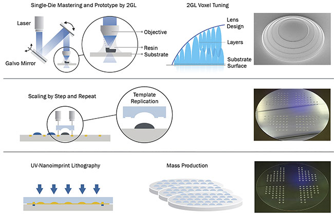
Figure 1. The full process chain — from single die to high-quality micro-optics — begins with two-photon grayscale lithography (2GL) mastering, is next scaled to wafer level by step-and-repeat (S&R) mastering, and ends with high-volume wafer-level manufacturing. Courtesy of EV Group and Nanoscribe.
Nanoimprint lithography
A major advantage of the UV-NIL process is that, for the final product, fully
functional optical structures or layers are transferred to the substrate. In this respect, the nanoimprint resist is the actual device, which potentially reduces the number of subsequent process steps. How-
ever, achieving this potential requires the NIL process to be scaled to the wafer level without compromising device quality. This, in turn, requires S&R mastering, which has proved to be a key enabling technology to achieve high-
quality products in high-volume, wafer-level manufacturing2.
S&R mastering is a UV-NIL-based
process comparable to the wafer-level UV-NIL process, in which an initial structure is replicated into a UV curing resin. The main challenge with the wafer-level process is that the master quality defines the success of subsequent production, so the quality of the initial single-die master must be preserved. Therefore, it is necessary to exactly replicate and place the single-die master hundreds or even thousands of times to produce masters for 200-mm or even 300-mm wafer production lines.
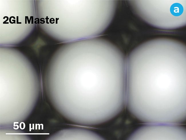
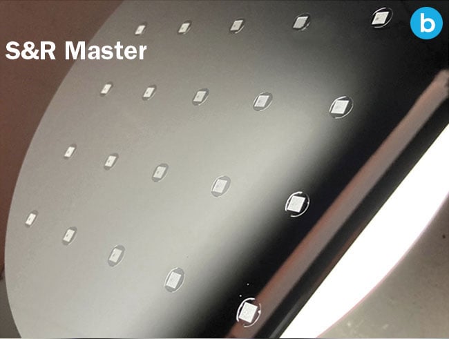
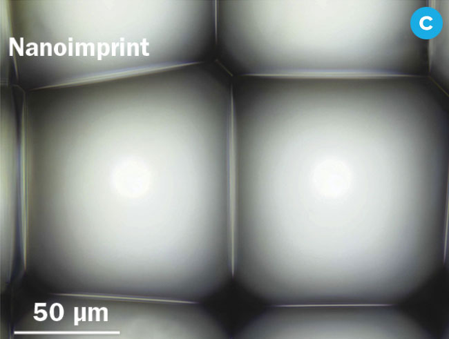
Figure 2. A 2GL master for diffuser optics (a).
A wafer-level diffuser master scaled by S&R (b).
Nanoimprinted diffuser optics (c). Courtesy of EV Group and Nanoscribe.
To support most advanced mastering requirements, the S&R system includes full process control, with precision alignment within 250 nm, and is capable of positioning every structure next to alignment patterns. All process steps — from dispensing, imprint, curing, and demolding — must also be performed precisely and monitored within a single environment to allow optimal feedback control. This not only avoids the impact of external sources such as airborne particles or temperature changes that
can lead to imperfections, it also enables the creation of both a wafer-level master with optimal quality and exact replicas
of every single die that can then be
applied to subsequent wafer-level manufacturing steps, ranging from the 2GL master prior to S&R (Figures 2a-2c). This process can be applied to the fabrication of a wide variety of structures, as shown in Figures 3a-3c.
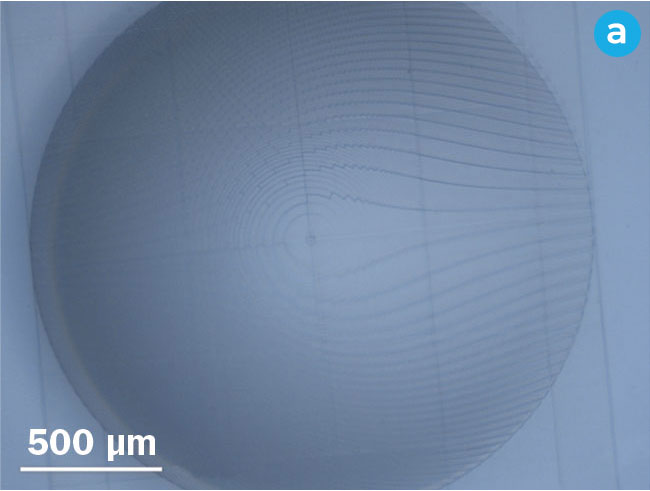
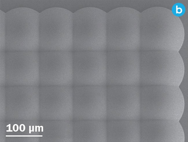
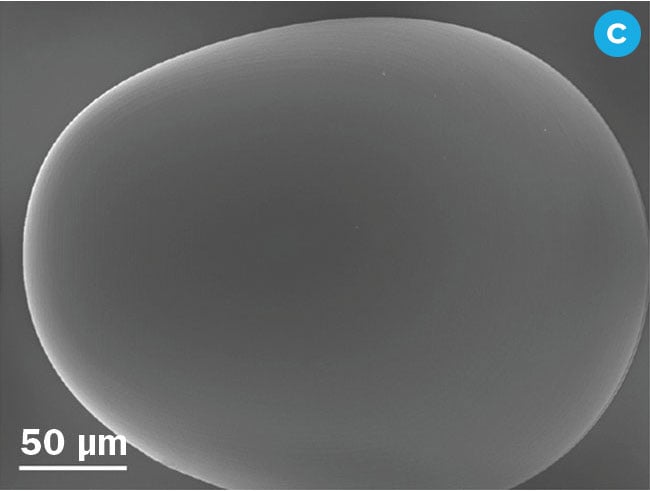
Figure 3. A nanoimprinted moiré lens (a). A microlens array (b). A freeform lens (c). Courtesy of EV Group and Nanoscribe.
During production, a working stamp is replicated from the S&R master and used for the actual imprint of the functional structure. This step is particularly useful for producing expensive masters because it minimizes wear and reduces the risk of introducing defects. Defective working stamps can be replaced quickly and at low cost, which can be particularly advantageous during high-volume production runs.
However, one consideration remains. With every replication step — from single die to S&R master to working stamp and final imprint — some changes in pattern dimensions are inevitable, due to shrinkage of the polymers caused by crosslinking during the UV curing process. These changes are predictable, some steps can even compensate for each other, and the deviations from the original design are very repeatable for a given set of materials. Thus, compensation can be calculated into the master design. Flexible fabrication methods, such as 2GL, support such design changes, as well as short iteration times.
Mastering with 2GL
The 2GL approach for additive manufacturing is capable of fabricating complex micro- and mesoscale topographies with submicrometer resolution in polymers that can either be used for replication or for direct investigation of the optical performance of single dies. Thus, it targets the needs of current optical
applications that require rapid microfabrication of freeform micro-optics, microlens arrays, and multilevel diffractive optical elements with the highest shape accuracy and optical-grade surfaces (for example, Ra ≤ 10 nm). These elements can then be transferred into mass manufacturing by using replication technologies such as NIL.
Innovative designs no longer require lengthy fabrication times, because such designs can be printed directly from a design file.
The 2GL approach is based on the simultaneous absorption of two photons by a photoresin3. This can only occur in a narrow focal volume of a femtosecond pulsed laser and results in a voxel, which can be imagined as a 3D ellipsoid ranging in dimension from ~160 nm (in the xy axes) and 500 nm (in the z axis), up to a few microns in scale. Scanning a laser focal point through the resin creates
freeform microstructures by overlapping
hardened volumes of these voxels and modulating each voxel on a 100-nm
grid and within more than 4000 height steps (gray levels). These degrees of freedom allow unprecedented freeform shapes (Figure 3c) and hybrid optics that combine diffractive and refractive features. This means that certain optical design requirements, such as eliminating dead zones while achieving sharp edges and high-shape accuracy, are no longer an issue. In contrast to classical grayscale lithography, 2GL comes without typical height limitations for features over
100 µm, and it provides excellent control of the surface topography. As an example, the moiré lens in Figure 3a consists of continuous spirals from 0 to 1.1 µm,
corresponding to a quasi-continuous
grayscale level. The diffuser in Figures
2a and 2c shows master and nanoimprinted templates of random freeform lenses over the whole printing area, and the microlens array in Figure 3b has a
filling factor of 100%.
Bridging the gap
By using 2GL to print freeform 2.5D master topographies with NIL as a precision replication technology, rapid prototyping becomes possible, and high-precision structures can be transferred to mass production. Innovative designs no longer require lengthy fabrication times, because they can be printed directly from a design file. The additive manufacturing process of 2GL, with its short design-iteration cycles, enables the production of NIL masters within a few days. The masters can then be directly tested for their quality and design, since optically clear resins printed on glass substrates allow direct testing of microlens arrays, hybrid lenses, and diffractive optical elements, as well as comparison from die to wafer level.
For traditional mastering methods, shape accuracy can be defined by metrology systems, such as confocal microscopes, surface profilers, or atomic force microscopes. Thus, the qualification of a prototype can be completed only after the entire wafer-level process is defined. With the combined 2GL/NIL approach, design validations can be completed early on, while the master is being created, and later verified for the production samples. Of course, these process steps are also applicable to other 2.5D structures and applications, such as sensor structures for microfluidic chips4.
In this way, new products can be developed in parallel, as shown in Figure 4. While the 3D-printed structure can be optimized for optical performance, a size-compensated master can help to optimize all required replication steps for wafer-level production. As a result, it is possible to quickly scale a pilot-line process while allowing flexibility for design iterations, enabling rapid time to market, and maintaining high flexibility for functional prototype designs.
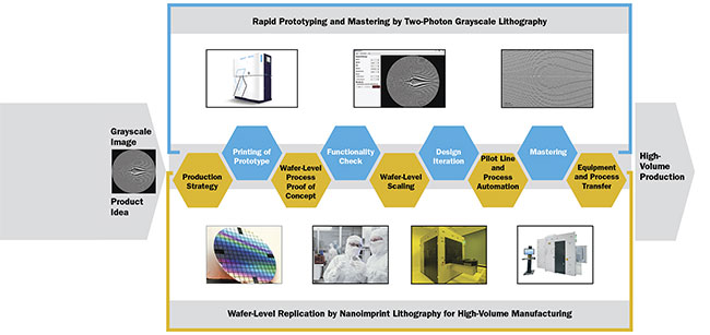
Figure 4. Quicker time to market is enabled by rapid single-die prototyping via 2GL 3D printing and the parallel development of high-volume manufacturing. Courtesy of EV Group and Nanoscribe.
The combination of two-photon grayscale lithography with nanoimprint lithography provides a new viable way to fabricate advanced optical designs. It enables new functionalities and provides a direct route to wafer-level manufacturing. This can overcome previous design constraints for micro-optical elements, including consumer products that require mass-production solutions, and can result in improved performance and new applications with innovative micro-optical designs.
Meet the authors
Martin Eibelhuber is deputy head of business development at EV Group (EVG), where he focuses on the application of EVG’s wafer bonding, mask alignment, and nanoimprint lithography technology in a variety of markets, particularly in compound semiconductors,
nanotechnology, and photonics; email: [email protected].
Jörg Smolenski is business development manager at Nanoscribe, where he is responsible for industrial 2PP applications such as mastering, integrated photonics (PICs), microfluidics, and many others. His expertise is in the area of 3D printing and laser technology; email: [email protected].
References
1. M. Eibelhuber et al. (February 2015).
Nanoimprint lithography enables cost-effective photonics production. Photonics Spectra, pp. 34-37.
2. C. Thanner et al. (February 2020).
Nanoimprint lithography for augmented
reality waveguide manufacturing. Proc SPIE, Vol. 11310, Optical Architectures for Displays and Sensing in Augmented, Virtual, and Mixed Reality (AR, VR, MR), 1131010.
3. Nanoscribe (2021). Introducing two-photon grayscale lithography, www.nanoscribe.com/whitepaper.
4. R. Sakalys et al. (2021). A reproducible, low cost microfluidic microcavity array SERS platform prepared by soft lithography from a 2 photon 3D printed template. Sens Actuators B: Chem, Vol. 340, www.doi.org/10.1016/j.snb.2021.129970.