Improvements in hardware and software, along with changes to camera sensor architecture, have enabled superior imaging in diagnostics and other life science applications.
MATTHEW KÖSE-DUNN, TELEDYNE PHOTOMETRICS
Most people are familiar with standard qualitative cameras and bright high-contrast images, thanks to the prevalence of increasingly powerful smartphone and digital cameras in the marketplace. Scientific-grade cameras, however, are designed to be quantitative, which means the technology can reliably determine photon intensities and detect low signals across large pixel arrays with the smallest degree of error and fewest artifacts, otherwise known as noise.
These capabilities have become increasingly relevant as scientific cameras have been put to use in more and more sophisticated situations, ranging from whole-organism light-sheet and super resolution microscopy to flow cytometry and voltage imaging of live neuronal signaling. These techniques have informed life science research and diagnostics in the realms of neuroscience (Figure 1), ophthalmology, genomics, and many others.
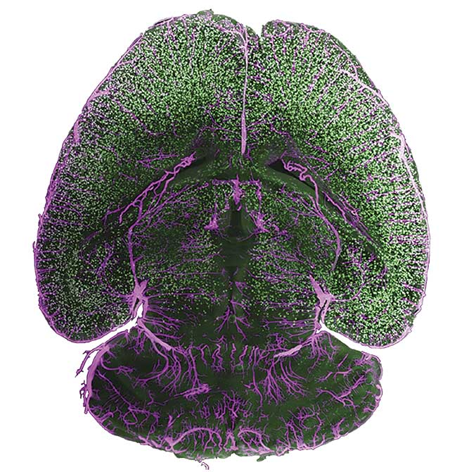
Figure 1. A cleared mouse brain. The image was taken with an Iris 15 sCMOS camera on a benchtop mesoSPIM (mesoscale selective plane illumination microscopy)
light-sheet system. The sample was stained for amyloid beta plaques (green) and arteries (magenta) and prepared by Anna Maria Reuss at University, Hospital Zürich. Courtesy of Teledyne Photometrics.
All cameras convert light into an image, and this process is shown in Figure 2. But a range of camera sensor architectures and technologies exists, along with huge variations in camera performance across major camera specifications — including sensitivity, resolution, speed, and field of view (FOV). In chronological order of development, the main scientific camera sensor types are charge-coupled device (CCD), electron multiplying CCD (EMCCD), scientific complementary metal oxide semiconductor (sCMOS), and back-illuminated sCMOS. It is useful to discuss these sensor types, their advantages and disadvantages, how camera technologies have improved over time, and how these advancements will benefit scientists in the future.
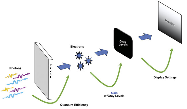
Figure 2. An illustration of the way an image is made by a camera. Photons are converted to electrons (split into pixels) by the camera sensor. The efficiency of this conversion is determined by the quantum efficiency. Electrons (analog) are converted to gray levels (digital) during readout, which is determined by the gain. The gray levels are then displayed as a monochrome image on the PC monitor. Courtesy of Teledyne Photometrics.
The creation of CCD sensors
The first working charge-coupled device was developed in the 1970s at Bell Laboratories1. But, although CCDs worked well for fixed samples with lots of signal (bright-field imaging of cells), these sensors struggled with moving, dynamic samples or low signals.
CCD cameras were typically slow
(~10 fps or less) and had a small FOV and low sensitivity because of their large read noise (up to 10 e¯ in some cases). While the small sensor size in CCD technology was mostly due to manufacturing expense, the inherent lack of speed was caused by a number of bottlenecks in their functionality. Having only one analog-to-digital converter (ADC) per sensor, for example, caused millions of pixels to be processed one by one. The electrons also had to be moved across the sensor below maximum speed to reduce read noise as much as possible, and the whole sensor had to be cleared before the next frame could be acquired.
Despite these disadvantages, CCDs have been integral in camera production for over 50 years, and they are still featured in a number of scientific applications. A benefit of CCD technology is its ultralow dark current (thermal noise that builds up over long exposures), often making CCDs the camera of choice for astronomy or luminescence experiments that require exposures in the range of minutes to hours. However, sCMOS technology has developed in parallel with the development of CCDs, and sCMOS sensors can now be integrated into long-exposure applications.
Either way, early CCDs lacked speed and sensitivity, leading to the development of a new technology — the electron multiplying CCD, or EMCCD.
EMCCD boosts capabilities
The first scientific grade EMCCD was developed in 2000, breaking new ground in both speed and sensitivity. EMCCDs are typically back-illuminated, which means that light can more efficiently reach the silicon camera sensor, resulting in increased sensitivity across a wide range of wavelengths. This capability, combined with the large sensor pixels (up to 24 × 24 µm), increased sensitivity and allowed for imaging of very weak signals, such as single-molecule or total internal reflection fluorescence experiments.
EMCCDs also use a gain register and the process of impact ionization to quite literally multiply the signal up to 1000× until read noise is no longer a barrier to digitizing an image. Due to this signal multiplication, these sensors can comfortably detect ultralow signals, which made EMCCDs the camera of choice several years ago for working with remarkably low signal levels, such as 10 e¯ or less.
Although EMCCDs were popular upon release, their advantages all came at a cost to other aspects of image processing. The large pixel size meant poor resolution and the need for very high magnifications (often over 150×), which further decreased an already small FOV under the microscope. And the electron multiplication process is temperature dependent, meaning it requires aggressive cooling (to around −80 °C) and careful electronic design. The process may decay over time (a factor known as EM gain decay), with increasing decay at higher multiplication levels. Experiments performed with a new EMCCD may not be comparable to experiments performed a year later with the same camera if it has been used regularly. Frequent camera calibration is necessary to maintain quantitative results. Finally, while EMCCDs can make read noise negligible, other sources of noise are multiplied along with the signal (for example, photon shot noise is increased by ~1.4×). This is known as the excess noise factor.
Today, EMCCDs are one of the most expensive formats of scientific cameras, and they have to compete with the capabilities of more recent sCMOS cameras.
Early sCMOS cameras
Although complementary metal oxide semiconductor technologies were technically in existence before CCD technologies, only in the 2010s did CMOS technology become more commonly used for scientific applications, making it often referred to as scientific CMOS, or sCMOS.
While CCDs and EMCCDs use similar sensors in their respective designs, sCMOS sensors are parallelized, as shown in Figure 3. CCDs and EMCCDs typically have a single ADC for the whole sensor, but sCMOS sensors feature miniaturized electronics on every pixel and an ADC for every column of pixels, resulting in a much faster readout. If a CCD or an EMCCD were visualized as a plane with a single exit for all passengers, then sCMOS sensors could be seen as a plane with an exit on every row. sCMOS cameras can image very fast, and electrons can be moved more slowly to drive read noise as low as possible, increasing sensitivity and allowing for the camera’s use in low-signal imaging applications, such as live-cell imaging and particle tracking.
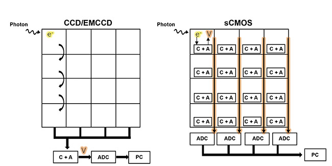
Figure 3. A comparison of the CCD and electron-multiplying CCD (EMCCD) sensor architecture versus the sCMOS architecture. CCD and EMCCD sensors have a single analog-to-digital converter (ADC) for the entire sensor, creating a speed bottleneck, while sCMOS sensors have an ADC for each column, allowing for parallelized imaging. The capacitor plus amplifier (C + A) converts electron volts to readable voltage. Courtesy of Teledyne Photometrics.
While CCD and EMCCD sensors can be expensive to manufacture, CMOS sensors have been adopted by the consumer electronics industry and are featured in virtually all smartphones and digital cameras, reducing the cost for making larger scientific sensors. CMOS sensors can also be constructed as large as needed for their use in microscopes and other imaging systems, meaning that sCMOS sensors typically have a much larger FOV than CCDs and EMCCDs, while also acquiring images at higher speeds.
However, although early sCMOS cameras featured higher sensitivity than CCDs, thanks to the lower read noise (~1 e¯ for sCMOS vs. ~10 e¯ for CCDs), EMCCDs have negligible read noise and could outperform sCMOS cameras in low-signal applications. Fast imaging regimes require low exposures and typically feature low signals, meaning that while early sCMOS cameras were fast, they often lacked the sensitivity needed to produce good image quality at high speeds. Developers of
sCMOS cameras had to increase the cameras’ sensitivity to compete with manufacturers of EMCCDs. This increase in sensitivity was achieved with the development of back-illuminated sCMOS.
Back-illuminated sCMOS
The first back-illuminated sCMOS camera, the Prime 95B, was developed by scientific camera company Teledyne Photometrics in 2016. Its back-illumination technology leads to a significant increase in quantum efficiency, from ~70% to 95%, as shown in Figure 4. The extra signal collection increased sCMOS sensitivity to a point at which it could compete with EMCCDs at low signal levels, as seen in single-molecule experiments and spinning disk confocal microscopy.
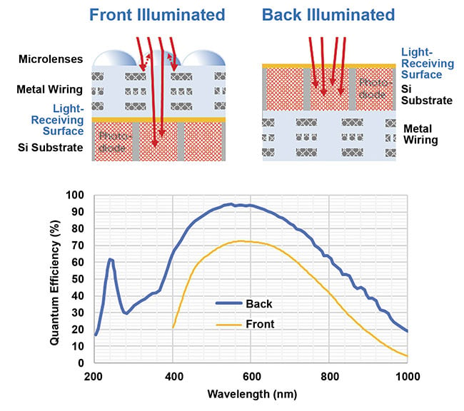
Figure 4. A comparison of front- and back-
illuminated sCMOS sensors. The sensor architecture (schematics). With front-illumination, light is focused onto the silicon (Si) by a microlens, which limits the quantum efficiency at a ~70% peak and passes through wiring and polymer. With back-illumination, the light immediately meets the silicon, which (due to having no microlenses) results in a much higher peak quantum efficiency and more sensitivity in the 200- to 400-nm range in the UV (graph). Courtesy of Teledyne Photometrics.
Back-illuminated sCMOS cameras feature all of the benefits of sCMOS technology (high speed, large FOV, and variable pixel size), along with sensitivity to rival EMCCDs, but with none of the traditional disadvantages (EM gain decay, excess noise factor, and expense). Back-illuminated sCMOS cameras have therefore been widely adopted by the scientific imaging community in recent years.
These cameras allow for some of the highest currently available peak quantum efficiencies (~95%), a clean bias (a lack of patterns or artifacts in the image), and huge improvements in the FOV and acquisition speed over EMCCDs and front-illuminated early sCMOS cameras. These benefits and improvements allowed researchers to image large, dynamic samples — such as embryos or organoids — at high speeds with high spatial resolution, all without sacrificing sensitivity and the signal-to-noise ratio. Due to the potential of back-illuminated sCMOS technology, in the years since its introduction, a new generation of sCMOS cameras has been developed that further increases the potential of the technology.
Next-generation sCMOS
Typical back-illuminated sCMOS cameras featured an FOV of ~18 mm diagonal, which could image at ~100 fps across the full sensor. These features, along with the high sensitivity and resolution that the cameras provided, were suitable for a wide range of applications in life science research, enabling the ability to capture large live samples with high image quality.
There were also additional applications that could benefit from a much larger FOV, such as light-sheet microscopy, and applications that required much higher speeds of about 1000 fps, such as voltage imaging, which is used to capture neural activity. Based on these needs, new sCMOS cameras have been developed that increase the speed and FOV together.
Some next-generation back-illuminated sCMOS cameras now have FOVs of up to 29.4 mm, as shown in Figure 5. This is more than twice the size of a typical sCMOS camera, and the newer cameras are able to obtain far more data per frame. Their 10-MP sensors require far more digitization and would typically result in a slower camera, but these next-generation sCMOS cameras also feature increased speeds — up to 500 fps across the full sensor — that are far faster than typical sCMOS cameras, while still imaging across a larger frame.
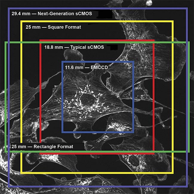
Figure 5. A scientific camera field of view (FOV) comparison. Although EMCCDs and typical sCMOS cameras are limited to smaller FOVs, next-generation sCMOS technology — with much larger FOVs, such as 29.4 mm — can capture more than twice the area. All measurements are made across the diagonal. Courtesy of Teledyne Photometrics.
Newer sCMOS cameras can now really push the limits of research. The cameras are able to image entire organs and directly observe neurons firing, and they even feature subelectron read noises. With the camera processor no longer a bottleneck, matching these cameras to a suitable microscope and PC becomes important. The microscope may limit the resolution and FOV that the camera can provide, depending on the optics. And the PC may limit processing rates, particularly when imaging 10 MP at 500 fps, which results in a data output of 5 GB/s. These sCMOS cameras can now image samples that were impossible to image with previously established technologies, outperforming everything that came before and moving the scientific imaging industry forward.
The future of sCMOS
As manufacturers continue to increase camera speed and FOV to capture still faster and larger samples, and to decrease noise sources until even single photons can be detected, other potential areas remain for which these technologies could be adapted.
Data storage. Faster and larger cameras will produce more data. Modern sCMOS cameras already push a 5-GB/s data rate. Since researchers often use multiple cameras at once, microscopy and imaging systems need to be designed to include consideration of the processing power, write speed, and storage space of the PC that the cameras are paired with. Although fast solid-state drive storage is now easily accessible, data often needs to be stored with redundancies in place, such as redundant arrays of independent disks (RAID), to ensure that no data is lost when acquiring or writing to disk.
These brute-force solutions can work — for example, for building a dedicated server for each imaging system — but data reduction methods must also be considered, such as using compression or imaging only the parts of the sensor that are relevant. Modern cameras include field-programmable gate array (FPGA) processors that can perform a variety of functions, such as compressing data as it comes off the camera or establishing multiple regions of interest in a sample and acquiring data only from those areas.
Another method to reduce image data size is to use 8-bit camera modes. Any data acquired in 8-bit mode will be half the data size compared to the more commonly used 12- or 16-bit modes. When imaging at high speeds or with low signals, 8-bit mode is more than enough to contain the image signal and produce high-quality images that are half the file size.
Smart imaging. Imaging algorithms have been developed in conjunction with camera technologies by using machine learning processes and AI data processing. Smart imaging allows for all sorts of image modifications. These include supersampling to increase resolution for the superresolution imaging of samples below ~200 nm in size, deconvolution to improve the signal-to-noise ratio of advanced imaging techniques such as spinning disk confocal microscopy, and even the automation of common image analysis for more high-content, high-throughput flow-cytometry or digital pathology applications. With a huge number of labs developing their own custom software and algorithms to solve specific problems, websites such as GitHub have become home to a massive range of open-source software to improve imaging alongside the hardware of the camera.
Additional dimensions and wavelengths. While most live science imaging occurs on 3D samples such as cells, tissues, or whole organisms, images produce 2D slices of the focal plane. 3D imaging — either through z-stacking, scanning, or special optics (such as light-field microscopy, which allows for a 3D image with every acquisition) — reveals more about a sample, including data that is more dense, complex, and challenging to process and present. 3D imaging will continue to become more prevalent, and cameras should be compatible with emerging techniques such as light-field microscopy.
While most imaging is performed within the visible range (~400 to 700 nm, the same range that the human eye perceives), imaging in the near-infrared (split into NIR-I at 700 to 900 nm and NIR-II at 900 to 1700 nm) has several advantages, such as less absorption and scattering, that allow for deeper image penetration into large samples. Effective use of NIR allows for the imaging of samples beneath the skin of an organism — which is useful for imaging and locating blood vessels in a clinical setting or for the imaging of live animals — and sensors will need to accommodate this part of the spectrum. The resulting imaging systems will have the ability to image into the center of 3D organoids or tissues in a nondestructive manner.
In addition, the lower energy of NIR photons allows for slower bleaching and longer timeframes in which to image. Although techniques such as two-photon microscopy allow for NIR imaging using standard silicon cameras, the quantum efficiency of these cameras drops sharply after 1000 nm. Longer wavelengths have even less scattering and absorption (and thus greater penetration), but silicon is transparent at these wavelengths. This is where alternatives to silicon sensors — such as indium gallium arsenide (InGaAs) sensors, which are sensitive from 900 to 1700 nm — can be used for techniques ranging from in vivo imaging of whole organisms for cancer detection and drug discovery, to characterization of NIR quantum dots and/or laser emissions.
These advancements are especially apparent in fields such as neuroscience, where larger, faster, and more sensitive scientific cameras have resulted in the field moving from imaging small groups of static, fixed neural cells to imaging live neural signaling activity from large populations, allowing for a deeper understanding of neural functions.
Scientific cameras are a vital part of life science and physical science research, and the technology has seen vast improvements over time, with the promise for new and exciting developments in the future. Samples that were historically challenging to image due to size, speed, or wavelength can now be easily acquired, providing more information and continuing to advance science.
Meet the author
Matthew Köse-Dunn is the content manager and applications specialist for Teledyne Photometrics, a scientific camera company. He has expertise in microscopy, life science research, and content generation. Köse-Dunn also hosts Teledyne Photometrics’ “Science Off Camera” podcast; email: [email protected].
Reference
1. M.F. Tompsett et al. (1970). Charge coupled 8-bit shift register. Appl Phys Lett, Vol. 17, pp. 111-115, www.doi.org/10.1063/1.1653327.