
The Integration of Materials in Photonic Chips
IVAN NIKITSKIY
From the perspective of conventional semiconductor manufacturers, there are several challenges to the integration of
photonic components on a chip. But perhaps the biggest challenge for photonic integrated circuits (photonic chips, or PICs) is that the demand faces an almost exponential growth in several market verticals, such as in fiber optics for data communications and telecommunications.
In microelectronics, scaling to meet growing demand was achieved by the now highly familiar silicon complementary metal-oxide semiconductor (CMOS) manufacturing technology. The maturity of CMOS manufacturing methods today makes it the semiconductor industry’s preferred method to fabricate everything. The very maturity and complexity of the CMOS process are what helped to improve the quality of many photonics products. The best examples are digital signal processors that clean up the performance of slow optics to provide high-level encoding for today’s increased data rates. The more complex an integrated electronic device technology is, the less the variety of technology platforms can sustain its growth.
A similar trend can be seen in integrated photonics. There are three major
material platforms with which to fabricate the components embedded in a PIC. Silicon, or silicon photonics (SiPh), and
silicon nitride (SiN) both use a conventional silicon wafer as a substrate on which to fabricate devices. The other
major material platform is indium phosphide (InP), a III-V compound semiconductor material.
These three main platforms for photonics integration are complementary. No single platform can serve all functions on a PIC. The key differentiator between the platforms is that only InP allows for the manufacture of active elements, such as lasers, in a photonic circuit. However, InP exhibits relatively high propagation losses when guiding the light signals, making it a poor choice for passive components, such as waveguides.
One downside of InP is that complex electronics are quite difficult to manufacture, in general — especially designs involving large-scale and very large-scale integration. Si and SiN elements, though they are more familiar manufacturing materials, do not support lasing or other active elements. However, these materials offer significantly lower light propagation losses, especially the SiN platform, which is even suitable for guiding the signals of single-photon emitters.
A Comparison of Manufacturing Methods for Integrating III-V Materials
Another differentiator is that the InP platform is only commercially available in 3- and 4-in. wafer formats, as opposed to the nearly 12-in. diameter silicon-based platforms available today. This affects the economies of scale for high-volume cost structures built on InP substrates.
The complementary nature of the three material platforms means that, eventually, the industry will seek to combine them in the most efficient way to fabricate highly complex PICs. The diversity of material platforms available to PIC designers is further multiplied by the variety of ways to integrate and package photonic circuits.
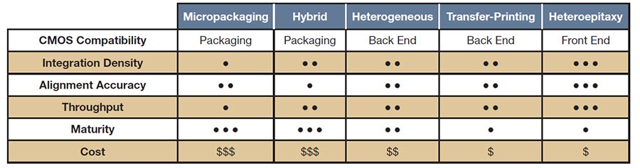
The most common methods for combining these material platforms in a PIC are summarized in the following table and described below.
Micropackaging is the among earliest approaches taken to develop silicon photonics. The technique couples an external laser in a micropackage to the waveguides in the silicon platform. However, the
complexity of this method grows significantly as the number of lasers increases
in a chip design, which eventually challenges the scalability of the platform.
Hybrid integration takes a different approach. Rather than coupling a silicon or SiN wafer to a laser, this approach combines the whole PIC in a III-V material platform, including a laser, an array of lasers, or an array of lasers with modulators. Hybrid integration is a broad term that is widely used by companies working on photonics integration. The most prominent example of its application at the foundry level is the Joint European Pilot Line for Indium Phosphide-Integrated Photonics, or JePPIX, which offers foundry services through the Fraunhofer Heinrich Hertz Institute in Berlin and through SMART Photonics in Eindhoven, Netherlands. Infinera, Lumentum, and other foundries also offer products based on InP materials that are suitable for hybrid integration.
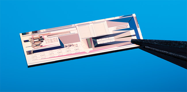
A photonic integrated circuit (PIC) on a chip. Courtesy of imec.
Heterogeneous integration is another manufacturing approach for bonding
III-V materials on top of silicon via
conventional die bonding. This technology is becoming very mature. CEA-Leti
and imec are actively exploring this
integration process, with imec moving
toward a new 12-in. wafer platform on phosphorous-doped silicon (SiP). Major silicon foundries — such as Intel, Juniper,
Advanced Micro Foundry (AMF), and Tower Semiconductor — exploit this method, despite that it requires a very specific process. Heterogeneous integration methods are easily scalable, but they require a major investment to build them from the ground up.
Wafer-scale heterogeneous integration creates III-V membranes that contain
native optoelectronics and submicron nanophotonic waveguide devices in the same layer. This technique is being explored jointly at JePPIX and Eindhoven Technical University. Such membranes can also be integrated on top of electronics, which enables the assembly of photonics and electronics at wafer scale using high density via interconnections fabricated with precision lithography.

Wafer-scale heterogeneous indium phosphide (InP) membrane integration. Courtesy of JePPIX.
Micro-transfer printing is another method that recently emerged from
academic developments. It implies fabricating coupons embedded with active devices and then scale-transferring them through a stamp at relatively large volumes so that multiple coupons can be transferred at the same time. The stamp is then aligned and bonded to a carrier wafer that contains passive circuitry, such as silicon or SiN waveguides. Transfer printing is a far more scalable approach than micropackaging. This integration technique has been among others
pioneered by imec, which is working
on key challenges, such as maintaining precise tolerances for stamp alignment.
Heteroepitaxy — often described as
the holy grail for the precise, scalable manufacture of highly complex PICs —
is still under development in academic labs worldwide. It involves the monolithic integration of III-V materials on silicon and promises low-cost yet large-scale manufacturing with high throughput, as well as accurate alignment, the efficient use of III-V materials, and potential compatibility with front-end silicon CMOS processes. Heteroepitaxy would further enable PICs that comprise multiple bandgaps obtained from selective area growth, regrowth steps, or intermixing of materials, as is done in the case of InP. Given its potential benefits, this process is an active area of research within academia as well as industry, with initiatives underway at AIM Photonics, imec, and NTT, among others. Many traditional CMOS foundries are also exploring epitaxial growth of III-V materials on silicon as a “more than Moore” technology (in reference to Moore’s law) to further extend the per-
formance scaling of transistors past what conventional silicon electronics can achieve by leveraging photonics.
Hybrid integration appears to be the approach to which many companies are dedicating resources in the near term. Meanwhile, apart from the three major PIC material platforms of SiPh, SiN, and InP, several novel PIC platforms open even more possibilities for the hybrid integration approach.
Barium titanate (BTO) is a material with a naturally high Pockels effect, which allows the material to be used for optical modulation. Lumiphase in Switzerland is developing the technology as a hybrid PIC platform based on silicon photonics.

A hybrid CMOS-silicon photonics transceiver prototype developed at imec. Courtesy of Imec.
Thin-film lithium niobate (TFLN) modifies the conventional lithium niobate material that has been used to make optical modulators for telecommunications networks since the 1990s. While the footprint or size of TFLN devices is larger than those fabricated from electro-optical polymers, TFLN can more easily leverage the maturity of semiconductor fabrication methods in the near term. HyperLight, based in Cambridge, Mass., is developing TFLN for high-speed optical modulation with electrical-optical bandwidths that exceed 50 GHz.
Electro-optic polymers enable 2- to
3× faster optical modulators than conventional material platforms. The polymer is used in liquid form, allowing it to boost the performance of solid-state semiconductors. Because the material is also organic, it can be easily implemented into silicon foundry processes for high-volume manufacturing.
Electro-optic polymers can enable higher-speed optical modulators that
operate below one volt of bias to be directly driven by on-chip electronics, avoiding the added expense of external drivers. The use of these materials reduces power consumption by lowering the voltage drive, and it allows electronic digital signal processing chips to be more power-efficient. Lightwave Logic in Englewood, Colo., is developing an electro-optic polymer platform for modulators that have already demonstrated over 100 GHz and 3 dB electrical-optical bandwidths.
Several material platforms will be needed to serve the growing volume and variety of integrated photonics applications. Currently, the hybrid integration approach to manufacturing devices is the most popular across the industry. But PICs completely contained within layers
of III-V materials that are grown on silicon using heteroepitaxy offer greater technological and economic advantages and potential performance. However, more time will be required for further improvement before heteroepitaxy can demonstrate functional photonic chips manufactured in high volume. Ultimately, no single material platform can cover all of the needs of a PIC designer. The target application will drive the choice of material platforms in photonic chips, while the manufacturing and cost requirements will determine which integration approach is used to fabricate them.
/Buyers_Guide/EPIC_-_European_Photonics_Industry_Consortium/c32606