Rapid advances in nanolaser research are making this area of photonics a very hot topic. Whether
tackling high optical losses in nanocavities or achieving room-temperature operation,
scientific groups worldwide are helping to bring the nanolaser closer to practical
operation.
Often, as science takes a step forward, it brings about new capabilities
in not just one field, but in a multitude of others – and these areas are
not always related to one another. This is particularly true when it comes to advances
in photonics technologies, which seem to have almost endless applications.
Nanolasers are no exception. Imagine a nanoscale optical laser,
so small but promising so many extraordinary advances in many fields. These types
of devices will bring new capacity to biosensing, data storage, photolithography
and optical communications. When compared with their larger cousin – the laser
– the biggest advantages of using nanolasers are their ultrasmall physical
size and mode volume as well as their ultrafast operational speed and low power
requirements.
Because of strong optical confinement in nanolasers, light-matter
interactions can be greatly enhanced, which means that very weak effects might be
observable. This could come in handy for detecting single molecules, enabling extremely
sensitive biodetection.
Nanolasers also can be used for ultradense data storage and high-resolution
photolithography. More importantly, they are the most promising on-chip photon source
for ultracompact, ultrafast photonic circuits.
Several groups are working on making nanolasers a useful and usable
reality. As a result, progress is advancing rapidly. Nanolasers now cover a wavelength
range of about 500 to 1400 nm, with footprints down to below 1 μm2.
Surface plasmons
In recent years, scientists have turned their attention to the
use of surface plasmons, rather than photons, for amplification in the laser cavity.
Unlike light, which cannot be focused down to a spot that is less than approximately
half its wavelength by conventional means, plasmons are spread over much shorter
distances and thus can overcome this diffraction limit.
Plasmons are generated when light is incident upon a metallic
surface. Free electrons at the surface of the metal interact with the electromagnetic
wave to form plasmons, which oscillate over the surface, resulting in laser light
emission.
The concept of the surface plasmon laser, or “spaser,”
was proposed in 2003 by professor David Bergman of Tel Aviv University in Israel,
who worked alongside Mark Stockman of Georgia State University in Atlanta. Together,
they presented the idea of the spaser in a paper published in Physical Review Letters.
They believe that any future nanometric optical or surface-plasma device will have
to include spasers for generating the appropriate signals.
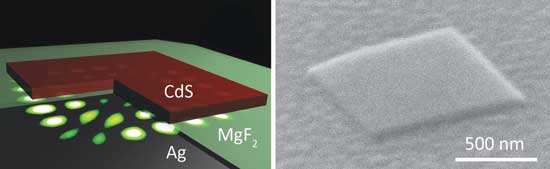
Left: Schematic of a plasmon laser showing a cadmium sulfide (CdS) square atop a silver (Ag) substrate separated by a 5-nm gap of magnesium fluoride (MgF2). The CdS square measures 45 nm thick and 1 μm long. The most intense electric fields of the device reside in the MgF2 gap. Right: Electron microscope image of the plasmon laser. Courtesy of Ren-Min Ma, University of California, Berkeley.
“Spasers will have to be used in nanophotonics and nanoplasmonics
as the source of the surface plasma waves or coherent quanta that will be modulated
or manipulated in order to process and transmit information in a nanoscale device,”
Bergman said.
Bergman and Stockman’s proposals were turned into reality
six years later and reported in a 2009 Nature paper by Mikhail Noginov, a materials
scientist at Norfolk State University in Virginia, and co-authored by Vladimir Shalaev
of Purdue University in West Lafayette, Ind., and Ulrich B. Wiesner of Cornell University
in Ithaca, N.Y.
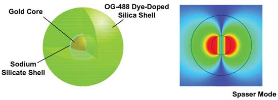
The smallest laser emitting visible light was built in 2009. It combines dye molecules
and gold nanoparticles within a silica shell to generate enough energy to produce
surface plasmon oscillations. The resulting laser light is emitted at about 530
nm. Courtesy of NSU-Purdue-Cornell.
The tiny laser combines dye molecules and gold nanoparticles within
a silica shell to generate enough energy to produce surface plasmon oscillations.
The resulting laser light is emitted at 531 nm – the smallest laser operating
in the visible.
For Shalaev, the significance of the nanolaser can be summed up
easily: The nanolaser is to future nanophotonic circuitry what the transistor was
to nanoelectronics. “There is great societal need to process information faster
and, with the current electronics, one can’t go faster than around 100 GHz.
Nanophotonics could process information much faster with a frequency which is limited
only by the carrying frequency (around 1015 Hz).”
Shalaev accepts that using dyes as the active medium could be
less than ideal for some applications when compared with the semiconductor gain
media used by other groups. But it seems that all of the nanolasers demonstrated
so far have pros and cons.
Nanolasers heat up
At the same time, in another Nature paper published in the same
year, a group at the University of California, Berkeley, presented a competing route
to the plasmon laser. The team, headed by Xiang Zhang, a professor of mechanical
engineering, reported a clever hybrid plasmon laser located with a 5-nm gap between
a semiconductor nanowire and a silver surface.
To operate properly, the plasmon laser had to be cooled to cryogenic
temperatures as low as 10 K. Such extreme cooling was necessary to produce the extra
amplification needed as a result of light leaking out of the laser cavity.
Blue light is emitted from the
first semiconductor “spaser” that runs at room temperature, instead
of in a cryogenic vacuum. This special type of nanolaser amplifies particles called
surface plasmons, which can be confined in smaller spaces than conventional light.
Courtesy of Ren-Min Ma, University of California, Berkeley.
Later, in 2010, the team figured out how to plug the leak, and
room temperature nanolaser operation was achieved.
Zhang’s team uses total internal reflection to confine the
plasmons within a nanosquare device. The laser, composed of a cadmium sulfide square
measuring 45 nm thick and 1 μm long, is placed on top of a silver surface and
separated by a 5-nm gap of magnesium fluoride.
Using this configuration, the emission rate of light was increased
eighteenfold and confined to around 5 nm.
By tackling the light leak, the team could do away with the cryogenic
chamber and opt for room-temperature operation instead.
On the road to practicality
Some challenges are inevitable when working with devices that
are so small, said Ren-Min Ma, a postdoctoral researcher in Zhang’s lab and
co-lead author of the Nature Materials paper. Perhaps the biggest challenge to their
practical use occurs when the laser light is emitted, he added.
“It is still difficult to integrate nanolasers into a device.
Firstly, the subwavelength cavity sizes result in strong divergence of emission
due to diffraction of light preventing collection of their emitted energy,”
he said. “Further, it’s also challenging to construct electronic interfaces
on them without disturbing the cavity modes or increasing the device footprints.”
If these problems can be solved, Ma believes that manufacturers
will readily adopt nanolasers for new applications.
Integration with Si-based circuits
Another important step on the road to commercial uptake was reached
earlier this year by professor Connie Chang-Hasnain’s group in the Department
of Electrical Engineering and Computer Sciences, also at UC Berkeley. The team found
a way to grow nanolasers directly onto silicon, bypassing the problem of forcing
together two different materials with mismatched atomic structures.
“Our research demonstrated a completely new growth mode
to obtain metastable, single crystalline compounds on highly lattice mismatched
substrates,” Chang-Hasnain said. “This opens the door to heterostructure
integration in a way that no way had done before, and the growth is initiated by
nanostructures.”
In a Nature Photonics paper published in February 2011, the team
describes how it grew indium gallium arsenide nanopillars onto the surface of silicon.
The small footprint of the III-V nanopillars meant that the constraints caused by
lattice mismatch could be avoided.
The researchers found that the nanopillars form a hexagonal crystal
structure, which results in a new efficient light-trapping optical cavity. The hexagonal
geometry allows light to circulate in a helical fashion up and down the structure,
enabling the signal to be amplified via this optical feedback mechanism.
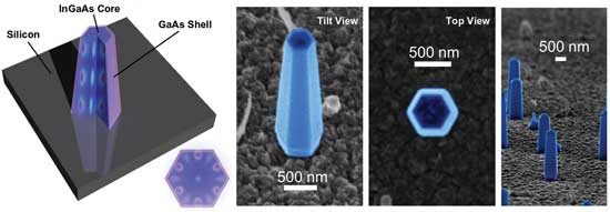
Connie Chang-Hasnain’s team
at the University of California, Berkeley, grew hexagonal nanopillars of indium
gallium arsenide (InGaAs) onto the surface of silicon, resulting in an efficient
light-trapping optical cavity. Courtesy of UC Berkeley.
And because of the low-growth temperatures, the lasers can be
integrated onto silicon after electronics fabrication has taken place in CMOS labs,
Chang-Hasnain explained. “Combined with the natural laser cavity provided
by our nanopillars, this has resulted in lasers on silicon, a critical component
needed in the future for silicon photonics.”
But an obvious drawback exists that has so far not been addressed.
For a nanolaser to be integrated into future electronic circuitry, it must be electrically,
not optically, pumped, as is currently the case.
“Electrically pumping our nanolasers is a critical challenge,
but one that we fully expect to solve,” Chang-Hasnain said. “The next
step would be coupling with already developed waveguide and detector technology
to establish optical links on CMOS chips.”
So when can we expect to see practical nanolasers make their debut
for use in the numerous applications that are waiting to benefit? For the man
behind the concept of the spaser, this is an exciting question.
“I do not know when the first practical spaser will be developed,”
Bergman said. “I hope and expect that it will happen soon because of the number
of groups who are trying to achieve this and because of the tremendous potential
applications of such a device in the future nanophotonic and nanoplasmonic information
handling technology.”
It may be some years before nanolasers become commonplace devices
on electronic chips, but in the meantime, they could be put to good use in other
areas; for example, they could enable single-molecule detection, allowing for extremely
sensitive biodetection.