Systems that use photonics to monitor the flow of liquid when assessing health can now capture a whole host of features quickly, accurately, and with increasing mobility.
As medicine and the monitoring of health have advanced into the modern era, researchers and clinicians have sought to capture an ever-increasing number of the biomarkers that are carried in biofluids, especially in biofluids such as blood and saliva that are present in living beings. Microfluidic systems establish a sterile environment in which to collect this information. Optofluidic components — including light sources, such as lasers and LEDs, detectors, lenses, and switches — have enabled these systems to reveal biomarkers that are essential to plotting a course for effective medical treatment, a capability that has become more important in a time rife with transmissible disease.
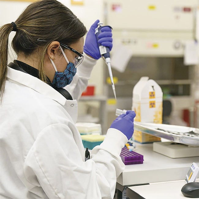
Figure 1. A technician delivers fluid for microfluidic analysis. Courtesy of LightDeck Diagnostics.
In simple terms, microfluidics involves the manipulation of a fluid — often a biofluid — in microscale systems to reveal certain inherent details about its composition (Figure 1). Optofluidics, a subset of microfluidics, is the use of photonic technology to capture these details. Typically, chips in which characteristics of biofluid are captured have been constructed using photolithography, which shines UV light through an opaque mask to produce specific geometric patterns in a layer of resist. These patterns are then made permanent on the substrate through chemical etching. Historically, the chips that house the biofluid were made of glass or silicon, but most are now made from a variety of polymeric materials.
As the components for microfluidics became smaller, these systems were able to fit into dimensions that could be placed on a desktop, said Giacomo Vacca, president of Kinetic River Corp. This works with companies that utilize the principles of microfluidics and optofluidics, but he said there have historically been limits to what can be miniaturized.
“There was always a trade-off, where manufacturers would miniaturize what they could and house it in a portable cartridge, and have the measurement components housed in a larger device that receives the cartridge,” Vacca said. “This prevents cross-contamination while ensuring that high-value measurement components are not thrown away after each test.”
Swift analysis
The rapid spread of COVID-19 has only accelerated the need for the mass production of microfluidic technology, along with requiring that tests be both efficient and fast, with results coming in hours or even minutes. The systems, along with their embedded photonics that reveal the traits of disease and infection in biofluid, are becoming increasingly portable. The day may soon come when such analysis occurs not only in medical clinics but also in nonclinical settings such as prisons and transportation hubs.
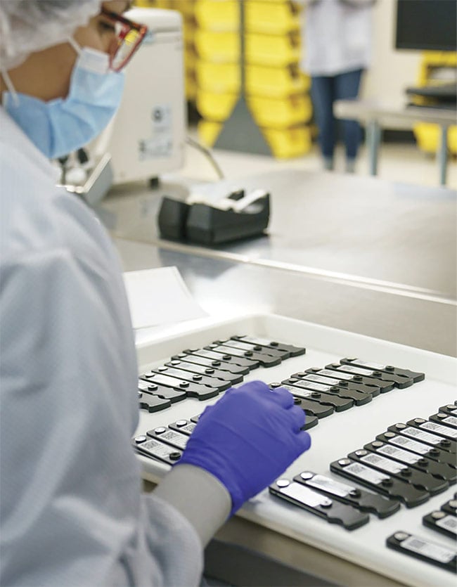
Figure 2. An array of organized microfluidic chips. Courtesy of LightDeck Diagnostics.
Enter the work of LightDeck Diagnostics. The company that has produced a multiplex imaging platform for quantitative whole-blood testing enabled by a planar waveguide and evanescent field illumination provided by a distributed Bragg reflector laser emitting at 640 nm. LightDeck Diagnostics produces disposable microfluidic chips (Figure 2) equipped with a microflow channel and an array contained within two fused plastic chips. The chips are placed in a small device where the fluorescence is detected, and tests are designed to be completed in 5 to 10 min in an environment outside the clinic or laboratory.
The company has received funding from both public and private sources, including the U.S. Department of Health and Human Services, to expand its production capacity as the COVID-19 pandemic has spread. But the company’s systems also apply to the detection of other diseases and conditions.
“Our technology has already been in use in water testing and veterinary medicine,” said Chris Myatt, chief innovation officer and founder of LightDeck Diagnostics. “It is capable of tracking 88 different features in the biofluid and is highly sensitive. In the old days, these test samples were sent to a lab and you’d get your results back in a few days.”
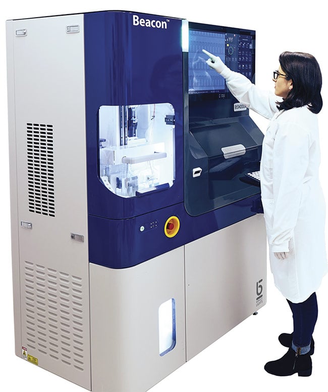
Figure 3. The Beacon technology accomplishes multiple tests on a small sample acquired through an optofluidic mechanism. Courtesy of Berkeley Lights.
The diode laser, housed in the small appliance where excitation occurs, is basically a red laser that minimizes autofluorescence and has characteristics similar to the laser reader in a DVD player, Myatt said.
LightDeck Diagnostics is working with manufacturers to produce up to 1 million tests a month. “Right now, we are focused on the professional market,” Myatt said. “But someday in the future, these devices could be in larger venues where you have to test a lot of people rapidly, as long as a technician was on hand who knew how to use the device.”
Interrogating cells
The foundation of optofluidics involves using light to isolate and identify cells according to their essential characteristics, to advance either scientific research or product development. Depending on the size of a sample being analyzed in an on-chip functional assay, it may be necessary to use light to manipulate the cells in question into their own chambers for quick individual single-cell testing.
Berkeley Lights’ technology makes this possible through a specially designed optofluidic system called Beacon, in which software helps to quickly identify and direct cells into so-called NanoPen chambers that are available in multiple sizes from ~300 pL to 1.7 nL. NanoPen chambers are nearly 100,000× smaller in volume than the typical test wells in a microliter plate. The mechanics of Berkeley Lights’ chambers allow the cells to stay healthy and grow, and the technology uses diffusion to remove waste and replace it with cell-sustaining nutrients. This allows the desired cells to be fully examined (Figure 3) based on such parameters as diameter, growth rate, surface markers, and secretion phenotype, without the dayslong duplication required by other assay methods.
“In a single NanoPen, we can interrogate single cells — up to 50 to 100 cells — and our chips have thousands to tens of thousands of these NanoPens,” said Keith Breinlinger, chief technology officer at Berkeley Lights. “The cells you are looking for make a particular protein. But, using traditional methods, you need to have hundreds of thousands or even millions of cells to detect the protein signal and find what you need.
“Many microfluidic devices use a continuous flow of cells moving past a detector illuminated by laser light, and they ‘see’ each cell for just a tiny fraction of a second,” he said. “What we do is deterministically put the cells together and perform biological experiments on them in the individual chambers and watch and interrogate them over a period of hours or days.”
In this way, data can be extracted at the single-cell level. For instance, the technology can interrogate the specific responses of T cells that originate in the thymus gland and that are an essential component in the immune system.
It is possible for this analysis to be almost entirely automated, Breinlinger said. The biggest sector that the company targets right now is the antibody therapeutic market, he added.
Berkeley Lights was co-founded by Ming Wu, a professor of electrical engineering and computer sciences at the University of California, Berkeley, to commercialize technologies that had been developed in his laboratory.
At the onset of the COVID-19 pandemic, the company worked directly with companies and researchers, such as those at Vanderbilt University Medical Center, who were racing against time to develop workable therapeutic antibody treatments or vaccines for the virus. The company also helped isolate the cells that were providing the most efficacious response, and it developed an antibody treatment that is now sold by AstraZeneca as EVUSHELD.
Monitoring drug efficacy
Some applications of microfluidics are moving past analysis to use the technology for continuous monitoring of biological processes, such as the study of the effectiveness of therapeutic drug regimens. The typical protocol for this monitoring is testing via repeated blood draws to identify any reactions that the body may have to the medicine, or to set potential changes in dosage needs.
In recent years, a group of researchers experimented with hollow submillimeter microneedles, with which they punctured the top layers of the skin of subjects and obtained small amounts of interstitial fluid (the body fluid between blood vessels and cells) to track the concentration of drugs such as the antibiotic vancomycin. Used to treat intestinal inflammation caused by bacteria, this medicine can incur side effects if not administered in the proper dosage. A microneedle was attached to an optofluidic mechanism based on a light absorbance system that consisted of a polydimethylsiloxane membrane and a waveguide that directed a
1 mW laser delivered through fiber optics. This system performed highly sensitive analysis of the fluid.
Most importantly, from the researchers’ perspective, this analysis could be accomplished without the need to transfer the sample to another chamber or piece of equipment, such as a chip-based assay or optical reader1. In time, the culmination of this technology could be a wearable biosensor.
“This information could be useful not only in drug discovery but also in stem cell therapies and tissue engineering,” said Victor J. Cadarso, a senior lecturer in the Applied Micro and Nano Technology Lab in the Department of Mechanical and Aerospace Engineering at Monash University in Australia. “When cells are stained for particular biomarkers, they might change behavior, and so that result does not necessarily reflect reality.”
Recently, Cadarso’s team has been working toward using this technology in disease detection, with experiments focusing on cancer organoids. The team is pursuing grant funding to further the technology’s development.
“In the end, this is about the creation of personalized medicine, where we can apply treatments and then track them, adjusting as needed,” Cadarso said.
Molecular-level discoveries
As the diagnostics and therapeutics that are made possible by microfluidic and optofluidic testing grow more sophisticated, applications including cell patterning, DNA analysis, and the analysis of biopharmaceutical products are expected to benefit. And as lab-on-chip configurations multiply and have increasingly integrated components, researchers and clinicians will be able to dive deeper into data extracted at the molecular level.
According to the market analyst firm Grand View Research, the demand for cell-based therapies is expected to drive a compound annual growth rate exceeding 16% through 2028. The potential for incorporating microfluidics and optofluidics components into wearable sensors is also driving research and development. Monitoring capabilities that once required a visit to a clinic or even a hospital stay could one day instead be performed remotely in real time.
These technologies could thus accomplish the twin objectives of making efficient and accurate testing available to larger numbers of people, while also tailoring treatment and care to the needs of patients who may have different reactions to the same illnesses and conditions.
Reference
1. S.A. Ranamukhaarachchi et al. (2016). Integrated hollow microneedle-optofluidic biosensor for therapeutic drug monitoring in sub-nanoliter volumes. Sci Rep, Vol. 6, No. 29075, www.doi.org/10.1038/srep29075.
Laser Seals Production
As microfluidic chips and the light-
activated mechanisms that they contain have evolved with more sophisticated diagnostic capabilities, so too have the prototyping processes that support the chips’ designs. For example, in the recent construction of an experimental prototype, a beam-shaping technique called multiplane light conversion directed 1030-nm femtosecond laser pulses (with a duration of 300 fs) through a series of phase plates to perform a precise weld of the polymeric materials in a microfluidic chip (Figure 1). The work was the culmination of a long-standing collaboration between corporate partners Cailabs and Lasea.
The femtosecond pulsed laser that was used can engrave the channels within a microfluidic chip (Figure 2), said Gwenn Pallier, a project and product manager at Cailabs. But when it comes to constructing a chip, beam shaping further provides a more secure seal between the polymer plates than could be produced by thermal or ultrasonic welding techniques.
Figure 1. A technique called multiplane light conversion is used to construct an ideal weld for microfluidic chips. Courtesy of Cailabs.
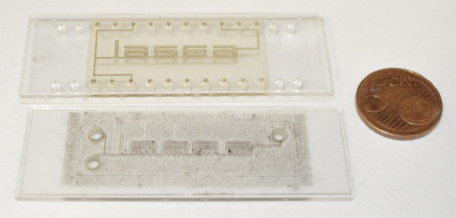
Figure 2. A comparison of a microfluidic chip welded with a Gaussian beam (bottom) versus one welded with beam-shaping technology (top). Courtesy of Lasea.
Marc Décultot, an R&D engineer at Lasea, said leakage could result from a bad weld.
The ability to establish a custom femtosecond beam profile also generates cleaner welds than a Gaussian laser beam could establish, fusing polymeric substrates together with less bubbling and cracking at the seam. The weld produced is also accomplished at a rate 9× faster than with a Gaussian beam, said Anne Henrottin, R&D manager in optical metrology at Lasea.
A sharp beam shape means that no energy is lost around the edges of the weld and that the beam will not damage the surrounding area, Cailabs’ Pallier said. A custom U-shape beam that has a diameter of 60 µm and is sharper than other beams, such as a Gaussian beam, is created by the multiplane light conversion technology, which is made of two mirrors with the light moving back and forth in between them.
Henrottin said the welding techniques developed at Lasea, with the focused beam on the microchannel edges, also prevent damage to the biological testing mechanism inside the microfluidic chip.
“We used a commercially available machine that allowed us to fire the laser while watching the results under a microscope,” she said. “The Cailabs module that performed the beam shaping was attached.”
The multiplane light conversion technology preserves the laser’s depth of field, unlike when laser beams are focused through diffractive optical elements.
Microfluidic chip manufacturers typically use a plastic injection molding process to mass-produce their chips, but this approach is too expensive and time-consuming to use when creating a prototype. Ultrashort-pulse lasers offer an alternative. They can be used for beam-shaping techniques that are applied to form microchannels in many kinds of transparent materials, including glass and silicon.
While the team is uncertain when its system will see widespread commercial use, Henrottin said the system can be fully automated, providing consistency once a particular chip design is chosen, and that it can be used to engrave, assemble, and seal microfluidic chips.
Building a Set of Standards
Since the formation of the Microfluidics Association two years ago, one of the association’s key goals has been to establish uniform specifications and a common vocabulary for various aspects of the microfluidics industry. A recently adopted standard put forward by the association was titled “ISO/CD 22916 Microfluidic devices — Interoperability requirements for dimensions, connections and initial device classification.”
“Besides that, we are working on test protocols for leakage test, surface qualification, dimensional control, optical transparency, and accurate measurement of fast-changing flow rates,” said Henne van Heeren, owner of enablingMNT and secretary of the association. “This has everything to do with quality control in production. When the industry agrees on a protocol, it will be transferred into ISO. The discussions take time, and sometimes the metrology has to be developed.”
The Microfluidics Association was founded in early 2020 and has 40 members who work in a variety of specialties, such as drug delivery, component supply, and lab-on-chip production (see chart).
Given that commercialization of a product takes an extended period of time, companies that hope for success in the industry need to find a niche that makes sense in the current marketplace. Standards help to limit the number of redesigns needed for a particular product, but many factors in the development process may merit standardization.
“Of course, the time to market depends on the application,” said van Heeren. “Research tools don’t need official qualification; they can go to the market quickly. Medical diagnostics take way longer.”
Nevertheless, some of the hottest applications in microfluidics include medical diagnostics, organs on a chip, and diagnostics for research, he said.
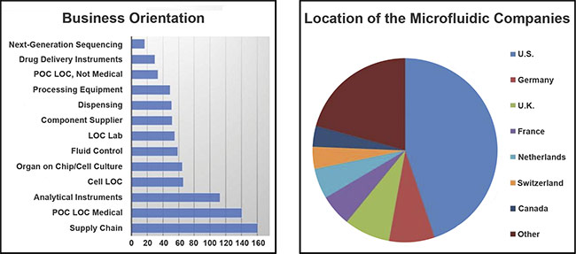
The various emphases of companies within the microfluidics industry (left) and the companies’ locations (right). Courtesy of the Microfluidics Association. POC: point of care; LOC: lab on a chip.
Different biomarkers, ranging from small particles to electrolytes, require different detection and measurement technologies. More often than not, more than one type of biomarker needs to be measured to produce an accurate picture of a disease or condition. This has led to increased specialization within the microfluidics market, all with the long-range goal of portability and hand-held modalities.
As with any technical industry, a flow of venture capital has helped to drive some products toward commercialization. In a presentation that van Heeren gave last year at the Microfluidics Symposium, he pointed out that many successful startup companies in the arena have been bought out by giants in the life sciences such as Agilent, Illumina, Bio-Rad, IDEX, Thermo Fisher Scientific, and Beckman Coulter. Each has acquired multiple smaller entities over the last decade.
For companies involved in the research and development of microfluidic technologies, the shift in energy and resources brought on by the COVID-19 pandemic has provided something of a tailwind: Both government and industry have sought to provide funding for development and commercialization of point-of-care technologies, for which microfluidics techniques are particularly well suited.
And while microfluidics techniques are more expensive than lab testing and lateral flow tests, the technology can provide quicker results and test several biomarkers simultaneously.
“Every professor claims that his or her developed device can be made cheaply by the millions, but the reality is different,” van Heeren said. “It is a fundamentally more expensive technology, but combining speed, accuracy, specificity, and/or multiplicity is an asset.”