Vertical-cavity surface-emitting lasers (VCSELs) differ from edge-emitting lasers in that their output beam is perpendicular to the top surface of the device instead of parallel to it.
L. Arthur D’Asaro, Jean-Francois Seurin and James D. Wynn, Princeton Optronics, Inc.
Unlike an edge emitter, a VCSEL has a maximum operating power that is not limited by catastrophic optical damage of the exit aperture because its aperture is larger and its PN junction does not intersect the surface in the region of high optical intensity. These and other advantages result in high reliability. VCSEL processing also has cost and yield advantages because testing can be performed while the devices are still in wafer form. Moreover, wafer processing lends itself easily to 2-D array fabrication.
Although VCSELs mostly have been confined to low-power (i.e., a few milliwatts) applications for optical data transmission, a few groups have demonstrated high-power (greater than 100 mW) devices emitting at around 980 nm.
At our company, we have developed them with a CW room-temperature output power of 3 W and an optical-to-electrical conversion efficiency of 25 percent. Additionally, the output power is emitted in a narrow linewidth (less than 1 nm) and in an inherently round beam. These 975-nm devices have a large active diameter of 350 µm.

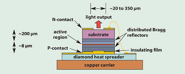
Figure 1. The structure of the high-power VCSEL features junction-down mounting on a diamond heat spreader to minimize thermal resistance.
The structure of the devices is shown in Figure 1, with some elements of the design omitted. They are grown by metallorganic chemical vapor deposition on N-doped GaAs substrates and are processed for bottom emission through the N-doped substrate material, which exhibits higher carrier mobility and lower free-carrier optical absorption than P-doped material. The devices are mounted upside down on diamond heat spreaders using AuSn solder. We have performed thermal simulations of our chip-on-submount design to optimize the design for efficient heat transfer and minimum thermal resistance.
VCSEL features
The properties of the P-doped distributed Bragg reflector are a limiting factor in the performance of a high-power VCSEL. Important characteristics are low series resistance to decrease heat generation, high thermal conductivity for efficient transfer of heat to the diamond heat spreader, and high reflectivity to reduce the threshold gain and increase the efficiency.1
It is difficult to achieve all three simultaneously, but several procedures involving bandgap engineering can be employed to lower the distributed Bragg reflector’s series resistance while maintaining a low doping concentration to reduce free-carrier absorption. Extensive modeling has been performed to optimize the number of pairs, layer composition and doping profile of the P-type distributed Bragg reflector of our devices.
We have designed the room-temperature offset between the peak gain wavelength and the cavity resonance wavelength so that they match at the elevated operating temperature. In addition, we have optimized the barrier height of the AlGaAs cladding layers around the quantum wells in the active region for high-temperature operation.
Some test results
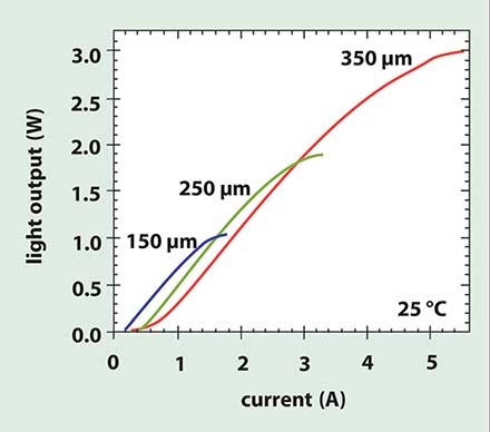
Output power measurements were performed on a temperature-controlled stage (set at 25 °C) using a calibrated integrating sphere with an extra output port connected by fiber to an optical spectrum analyzer. Figure 2 shows the light output vs. current characteristics for devices of different diameters, defined as the diameter of the P-contact in Figure 1. The output of 3 W is significantly higher than has been obtained by other groups.2,3

Figure 2. Light output vs. current at 25 °C for devices of different diameters (i.e., the diameter of the P-type contact in Figure 1) reveals a direct relationship between diameter and output power, up to 3 W in a 350-μm-diameter device.
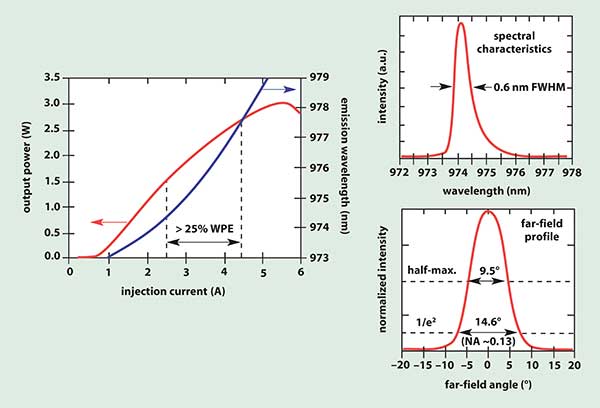
The data graphed in Figure 3 shows a wall-plug efficiency of more than 25 percent even for the large, 350-µm-diameter device. The device exhibits a reasonably stable wavelength across the operating range, which could eliminate the necessity of an external element for wavelength stabilization, as in some edge emitters. The spectrum remains relatively narrow (less than 1 nm FWHM) across the operating range. Far-field measurements of the multimode beam show a full-width 1/e2 divergence angle of about 15° and a Gaussian-like profile throughout the operating range.
Besides the advantages in reliability, the operating power density of high-power VCSELs is lower than for edge emitters because of their much larger emission area. Preliminary aging of our devices for 2500 hours under operating conditions at 70 °C showed no degradation. The failure rate (FIT rate) for high-power edge emitters is about 500, while that for low-power telecom VCSELs is less than 10, which is expected to be the case for high-power VCSELs as well.

Figure 3. Tests of a 350-μm-diameter VCSEL at 25 °C reveal a wall-plug efficiency (WPE) of more than 25 percent, reasonably stable wavelength across the operating range, a relatively narrow spectrum and a Gaussian-like profile.
Further development will lead to significantly higher power and efficiency. The straightforward implementation of 2-D arrays, characteristic of VCSELs, is expected to make the achievement of high powers relatively convenient. Near-term goals include a CW output power of 80 W and a wall-plug efficiency of 65 percent. Modeling indicates that we can achieve the higher efficiency by decreasing series resistance and threshold current. Longer-term goals are for 500-W arrays that have a wall-plug efficiency of 80 percent.
References
1. M.G. Peters et al (November 1994). Growth of beryllium doped AlxGa1–x As/GaAs mirrors for vertical-cavity surface-emitting lasers. JOURNAL OF VACUUM SCIENCE AND TECHNOLOGY B, pp. 3075-3083.
2. M. Miller et al (2000). Large-area high-power VCSEL. Proc. IEEE 17th International Semiconductor Laser Conference, pp. 63-64.
3. A. Mooradian (2001). High brightness cavity-controlled surface emitting GaInAs lasers operating at 980 nm. Proc. Optical Fiber Communication Conference 2001, Vol. 4, PD17-1-3.