High-quality thin films of BaZrS3 chalcogenide perovskites, developed by an MIT research team, show promise as a new semiconductor suitable for a range of applications, including solar and green lighting. The MIT researchers made the prototypical chalcogenide perovskite in a crystal structure of barium, zirconium, and sulfur.
Professor Rafael Jaramillo, who led the research, said that variations of the perovskite can be created by changing its composition, which lays the groundwork for development of a family of materials for use as semiconductors.
The researchers grew the films using molecular beam epitaxy (MBE) — a challenging technique, but one that allows crystal growth to be controlled at the atomic level. During MBE, a beam of molecules is pointed at atoms that are arranged on a substrate. The specific arrangement of the atoms provides a template for the molecules to follow as they grow.
“That’s why epitaxial growth gives you the highest-quality films. The materials ‘know’ how to grow,” Jaramillo said.
Using a single-step MBE process, the researchers created thin films of chalcogenide perovskites that exhibited atomic-scale smoothness, near-perfect BaZrS3 stoichiometry, and an atomically sharp interface with the lanthanum aluminate (LaAlO3) substrate.
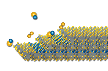
Artist’s conception of the epitaxial growth of a chalcogenide perovskite thin film. Variations of the perovskite can be created by changing its composition, which lays the groundwork for development of a family of materials for use as semiconductors. Courtesy of Felice Frankel.
The researchers grew the films by means of two growth modes. They used buffered epitaxy with a self-assembled interface layer to relieve the epitaxial strain and direct epitaxy. The latter mode allowed rotated-cube-on-cube growth to accommodate the lattice mismatch between the oxide substrate and the sulfide perovskites.
The chalcogenide perovskite thin films are made of inexpensive, nontoxic elements and are highly stable. “The thin films show a mirror-smooth image as a result of an atomically flat surface and excellent quality,” said professor Hideo Hosono at the Tokyo Institute of Technology. Hosono was not involved in the work.
“Now that we can make these high-quality materials, there’s almost no measurement we could do that wouldn’t be interesting to a wide community of people,” Jaramillo said. The MIT team aims to better understand the materials and aims to integrate them into solar cells.
The development of high-quality chalcogenide perovskite films has been achieved via pulsed laser deposition; Jayakanth Ravichandran, a colleague of Jaramillo’s and a professor at the University of Southern California, took the approach. Ravichandran and his team used pulsed laser deposition to trigger direct epitaxial thi- film growth of the chalcogenide BaZrS3.
Films resulting from Ravichandran’s study indicated that BaZrS3 thin films could be suitable for use as ultrathin front absorbers in tandem solar cells.
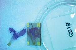
A blue flower is reflected in a thin film of a new semiconductor material developed at MIT. The clarity of the reflection testifies to the high quality of the film. Courtesy of Jaramillo et al.
The work of the Jaramillo and Ravichandran groups opens opportunities for high-quality chalcogenide perovskite thin films to be used in photovoltaic and optoelectronic applications.
Development of chalcogenide perovskites as a family of semiconductors, with properties that can be tuned with strain and composition in high-quality epitaxial thin films, has the potential to influence multiple other fields of technology, Jaramillo said.
“The history of semiconductor research shows that new families of semiconductors are generally enabling in ways that are not predictable,” he said.
The research of Jaramillo et al. was published in Advanced Functional Materials (www.doi.org/10.1002/adfm.202105563).
The research of Ravichandran et al. was published in Chemistry of Materials (www.doi.org/10.1021/acs.chemmater.1c02202).