Shrinking Pixels Improve IR Surveillance.
Arthur Stout, Electrophysics Corp.
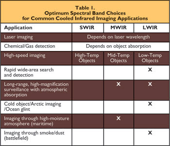
The demands of military electro-optical systems designers who require the detection of very small infrared signals over a wide variety of applications are driving advances in the area of 2-D photovoltaic infrared focal plane array (FPA) design and fabrication. The choice of the detector’s spectral sensitivity range often depends upon the application and is generally one of three bands: short-wavelength infrared (SWIR), medium-wavelength infrared (MWIR) and long-wavelength infrarec (LWIR). (See Table 1.)
Because of the requirements for high-sensitivity detection in these spectral bands as well as the capabilities realized with dual-band and two-color detectors, significant effort has been placed on decreasing FPA pixel pitch. Some of the expected primary system improvements include a reduction in cost and size, an increase in resolution and standoff performance, and improved reliability.
Although the path leading to the development of small-pixel FPAs for visible imaging has been well documented, there are significant and unique challenges facing the developers of IR photovoltaic imaging sensors.
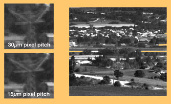
Figure 1. Shown is a comparison of 15- and 30-μm zoom images with the same optics. On the left, top 30-μm pixel pitch; on the bottom left, 15-μm pixel pitch. Right, original scene.
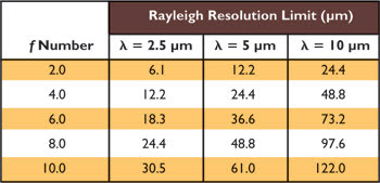
The impact of diffraction on image resolution is one consideration. To ensure diffraction-limited performance (see sidebar), systems design considerations require that the lens f number be appropriate in light of the IR wavelength band and pixel size; for example, an MWIR lens with an f number of 2 would be required to deliver an image with a resolution-limited performance of 12.2 μm. As the f number increases, the resolution worsens, with the limit increasing proportionally.
Besides the considerations relating to the limiting resolution, a variety of fabrication challenges exist. Today’s photovoltaic IR detectors are hybrid devices – silicon readout circuits welded to infrared detector arrays – and are fabricated using materials such as mercury cadmium telluride (MCT) and indium antimonide (InSb) for the MWIR and LWIR bands and indium gallium arsenide (InGaAs) for the SWIR band. A number of theoretical and fabrication limits exist to reducing pixel geometries in infrared imaging arrays.
Reconnaissance and targeting
Situational awareness is a key objective of systems engineers developing the next generation of infrared cameras. One important area is airborne imaging; for example, the increasing use of unmanned aerial vehicles (UAVs) for both reconnaissance and targeting has placed a greater demand on improving resolution. Payload constraints based on the airframes’ lifting abilities and flying time restrict the size of infrared optics. Smaller-pitch FPAs permit the use of smaller optics while maintaining the desired focal length and f number. Another example is in aircraft threat warning systems, which need a large field of view and high resolution so that systems can scan panoramically while maintaining the ability to detect a rocket motor firing at distances required to take defensive measures. The demands for detection range and large field of view can be accomplished only by reducing pixels to their diffraction-limited geometries.
In fabrication, a key concern is mastering hybridization technology for very small detector pitch size. Some manufacturers have found solutions, including Sofradir of Grenoble, France, which has pioneered a hot welding indium bump process that has achieved a very high yield of interconnection in megapixel arrays operating in the MWIR band with a 15-μm pitch. The hot reflow technology results in a very stable welding of the silicon readout circuit to the MCT detector, with the advantage of self-positioning of the two arrays by using the capillary forces of the liquid indium. Moreover, it enables simultaneous multiple array hybridization on a single silicon wafer, leading to a collective infrared FPA manufacturing approach suitable for very large array manufacturing.
In addition, fabrication of the silicon readout multiplexer is constrained by the die-size limits of photolithography systems, creating limits in increases of pixel resolution without reduction in pixel geometries. Today, 1280 × 1024-format arrays with 15-μm pixel pitch are in regular production at Sofradir.
Thanks to the planar MCT technology and good control of the diode implantation, the intrinsic performance of a 15-μm pixel is similar to that of 20- or 30-μm pixels. The 15-μm sensitivity is close to BLIP (background-limited infrared performance), and the MTF is measured at close to its theoretical value. The fill factor of the 15-μm pixel is measured at higher than 90 percent, whereas the crosstalk is lower than –30 dB.
The third generation of IRFPA sensors is expected to deliver multicolor or multiband capability, higher resolution, higher frame rates and better thermal resolution.
The primary requirement of the detectors is spatial coherence, which enables each pixel to detect various colors while requiring only a single connection (one indium bump per pixel). There are a number of programs now developing 1280 × 1024 two-color sensors with MWIR (3 to 5 μm) and LWIR (8 to 10 μm) spectral response. Their goal is to extend the range at which targets can be detected and identified. Target identification is important because US Army rules of engagement now require identification prior to any offensive action.
Because third-generation sensors will be megapixel devices with a physical surface of approximately 3 cm2, high-quality wafers will be needed to control processing costs. The transition from liquid phase epitaxy to molecular beam epitaxy processing of MCT arrays is a major goal in reaching regular production of cost-effective high- quality large-format detectors.
One advantage of molecular beam epitaxy versus liquid phase epitaxy layers is their composition and thickness uniformities, which are better and intrinsically linked to the low-temperature-evaporation growth technique. This has a major effect on the response uniformity and on the residual spatial noise patterns, which are significantly improved.
Another necessary processing advance for small-pitch pixel fabrication is dry etching of mesa structures. Wet etching is a very soft process that prevents MCT surface degradations, but this isotropic etching is inconsistent with the high fill factor in sub-20-μm pixels. Anisotropic plasma etches using ICP are now being used on pilot production processes and appear to be the best way to achieve both a low degradation of the material and sharp deep trenches in MCT epitaxial layers.
The demands for third-generation two-color infrared focal plane arrays are driving advances in fabrication processes, pixel structures, readout design and packaging. The current near-term benefits of small-pitch IR imaging array pixels are lower costs for 1/4VGA (320 × 240) and VGA (640 × 480) imaging arrays, viable commercial availability of megapixel (1280 × 1024) IR imaging sensors, lower power consumption, and improved performance and reliability in single-band mid-wavelength imaging systems.
Meet the author
Arthur Stout is vice president of business development at Electrophysics Corp. in Fairfield, N.J.; e-mail: [email protected].
Diffraction Considerations
Diffraction limits the resolution possible with an objective lens. In many optical lens calculations, ray-tracing approximations are made where electromagnetic radiation is approximated as traveling in straight lines from object points to image points.
In reality, diffraction spreads each point in the image to a spot whose size depends on the f number of the lens and the wavelength of the radiation. This pattern is called an Airy disk, and its diameter is given by the formula Airy disk diameter:
DAiry = 2.44 × λ × F
where DAiry is the diameter of the inner bright spot (see figure), λ is the wavelength of the radiation and F, the lens f number.
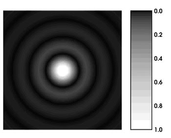
Figure 1. Impact of diffraction on image resolution.
For a well-corrected objective lens with a uniform circular aperture, two adjacent points are resolved when the centers of their Airy patterns are separated by a minimum distance equal to the Airy disk radius:
Rayleigh resolution limit = DAiry/2 = 1.22 × λ × F.
This equation describes the minimum distance between the centers of the Airy patterns. At the diffraction limit, typically about 20 percent of the focused energy must be captured by the detector pixel, limiting the size of an infrared pixel to twice the wavelength being detected. The remaining 80 percent of the radiance is split between at least eight surrounding pixels.
The table shows how the Rayleigh resolution limit varies with the lens f number for several infrared wavelengths. As shown, an f/2 infrared lens delivers an image having a resolution limit of 12.2 μm for 5-μm radiation. As the f number increases, the resolution limit increases proportionally.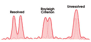
Figure 2. Airy pattern distribution.
When considering the development of smaller-pixel FPAs, a question arises: Are pixels that are smaller than the Rayleigh resolution limit somehow worse? Not necessarily. Even if the Rayleigh resolution limit is reached with larger pixels, an image obtained with smaller pixels will not be any worse. Both scenarios still have the same total resolution, although one will produce a larger stored digital image.
 And even though the resolution is the same, a camera with smaller pixels will render an image with fewer artifacts, such as moiré and aliasing. Smaller pixels also provide the flexibility of having better resolution with larger apertures, in situations where the depth of field can be shallower. When other factors such as noise and depth of field are considered, the answer as to which is better becomes more complicated.
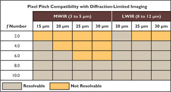
It should be clear from the table that, to produce infrared images with the highest possible resolution given a desired focal length – i.e., field of view – systems designers should select the fastest possibleobjective lens – with the lowest f number – and a detector with the smallest available pitch. The chart defines what is required to achieve diffraction-limited imaging of these fast imaging systems. With increasing optical f numbers, because the Rayleigh resolution limit distances increase, most of the common detector pitch values will be sufficient.