Quantum dot deposition technology continues to evolve, allowing for tunable and scalable sensor devices that offer versatile new design options for the shortwave infrared band and beyond.
CONG-DUAN VO, STUART STUBBS, AND HAO PANG, QUANTUM SCIENCE LTD.
As a second quantum revolution begins, many
mysteries remain in the quantum realm. Perhaps this is unsurprising given the notoriously confounding properties of this new frontier. However, as time passes, it seems increasingly likely that the development of new technological advancements and applications depends on understanding these mysteries.
For example, quantum technology could enable a generational leap forward in near-infrared (NIR) image sensors, and particularly in shortwave infrared (SWIR) image sensors, which are currently dominated by indium gallium arsenide (InGaAs) technology. The use of InGaAs is prohibitively expensive for many applications.
Quantum dot photodiodes have the potential to be much more compact than equivalent technologies, making them more suitable for commercial applications.
It is fitting that the key to overcoming this huge challenge comes as a tiny solution: quantum dots (QDs).
Quantum dots have already found
application in consumer display technology and medical science. Recent breakthroughs in SWIR-sensitive quantum dots suggest that they could herald a generational leap in imaging applications and sensing.
As nanoscale semiconductors, quantum dots behave in a way similar to naturally occurring atoms in that QDs confine electrons and electron holes within a three-dimensional space. One effect of this
confinement becomes evident when a photon of light carrying more energy than the bandgap of the quantum dot is incident on the QD’s surface. This occurrence excites one of the quantum dot’s electrons to a state of higher energy, prompting it to leap from the valence band to the conductance band. In effect, the electron is “knocked” out of its hole by the photon. To return to its hole, the electron must release energy by emitting light. The wider the gap, the more energy it takes to cross it.
Conventional IR sensor challenges
Two material technologies currently deliver the level of performance required for SWIR sensing applications: InGaAs and silicon germanium (SiGe). Both come with significant drawbacks. Of the two, InGaAs sensors are the most prevalent and are more mature.
InGaAs sensors are commonly used for machine vision applications. Camera technology based on InGaAs photodiodes
operating within the 0.9- to 1.7-µm
SWIR region offers high detection
performance, high quantum efficiency, low dark current, fast response speed, and excellent reliability. Extended
InGaAs alloys using higher InAs
composition can detect wavelengths up
to 2.6 µm. However, these materials
tend to have more defects in batch
production. The resulting production inefficiencies reduce device performance and exponentially increase production costs.
The high fabrication cost, low throughput, low pixel resolution, and bulky design of InGaAs sensors make the technology impractical for use in consumer electronics. The high cost and limited pixel size and resolution of InGaAs sensors stem from the intricacy of the
fabrication processes: InGaAs is epitaxially grown on indium phosphide (InP) wafers and then diced into chips before the array of individual InGaAs chips
are bonded with silicon readout integrated circuits (ROICs) via flip-chip hybridization bonding. This complex fabrication method makes it challenging to scale up the process on large InP wafers due to the very fragile nature of InP materials and the difficulty of manufacturing the large wafers.
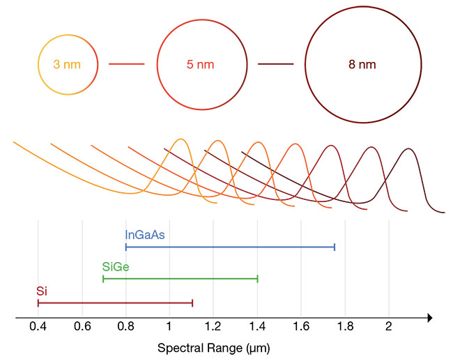
Quantum dots that are fabricated to be between 3 and 8 nm in size allow the development of sensors with tunable wavelengths across the NIR to SWIR bands. Courtesy of Quantum Science Ltd.
Advanced InGaAs sensors using copper-to-copper hybrid wafer bonding technology can achieve scaling of pixel pitch down to 5 µm, allowing for high pixel density and resolution1. However, susceptibility to dark noise from high dark current at room temperature requires InGaAs sensors to be deeply cooled to achieve adequate image quality. The need for a cooling system adds significant bulk to the end product.
InGaAs technology, therefore, is only used for niche markets such as military, aerospace, and demanding inspection equipment applications, for which cost-effectiveness is a lower priority.
Sensors based on SiGe materials technology, in contrast, directly integrate germanium photodiodes onto silicon
wafers. SiGe technology enables high-speed and low-cost IR image sensors. However, their high dark current and
limited light detection range (typically up to 1.6 µm) impede market penetration. Other drawbacks are that a thick active layer is needed to absorb longer wavelengths and that space is required when using silicon and needing to integrate SiGe photodiodes into ROICs. SiGe
technology is more appropriate for
surveillance, industrial automation, and
diagnostics applications that must compromise between device performance
and cost.
InGaAs and SiGe are useful for certain applications, but neither has all the
qualities needed to enable a generational leap in sensing technology. A recent report by Yole Développement on SWIR imaging suggests that a more complete solution could produce a paradigm shift
in the sector2. The report predicts that high-performance solutions will begin to replace legacy technology by 2027, with the main trend being the emergence of
the quantum dot.
More than a material solution
Colloidal quantum dot (CQD) image sensor technology is a rapidly emerging solution for delivering image sensors with spectral response spanning the ultraviolet, visible, near-NIR, and SWIR regions of the spectrum. These sensors offer high detection performance and high resolution. Importantly, quantum dot-enabled sensors achieve this for a fraction — 1% to 0.1% — of the cost of legacy SWIR technology.
The technology integrates a CQD-based pixel stack onto a CMOS ROIC at wafer scale. Unlike conventional IR light absorbers, such as SiGe and InGaAs, that are generally prepared using costly high-temperature processing under high-vacuum conditions, CQDs are typically produced using wet chemistry. This facilitates manufacture on a large scale.
The unique wavelength tunability of quantum dots in a wide spectral range is achieved by controlling the size of the nanocrystals. This tunability — along with strong optical absorption, large dielectric constant, and small exciton binding energies — makes these nanoparticles ideal as the active IR layer for image sensors. In addition, their solution processability and their compatibility with diverse substrates and form factors make CQD technology promising for widespread scalability.
Scalability makes supplying the volume of SWIR-tuned quantum dot sensors more feasible for a range of new applications. These more easily scalable sensors could provide cost-effective solutions for detecting crop quality and bruising on fruit, identifying defects in silicon wafers, detecting black ice on the roads, and even evaluating conditions beneath the skin for medical applications.
SWIR Vision Systems, Emberion, STMicroelectronics, and Imec have all introduced CQD imaging devices for industrial use as alternatives to InGaAs-based technology. CQD image sensors have been used in devices demonstrating small global shutter pixels of less than 2-µm pixel pitch. These image sensors, delivering high performance and substantial reductions in production costs, unlock new application opportunities.
Consistent, fast manufacturing
As with any groundbreaking technology, quantum dots pose new challenges for sensor and imaging systems designers.
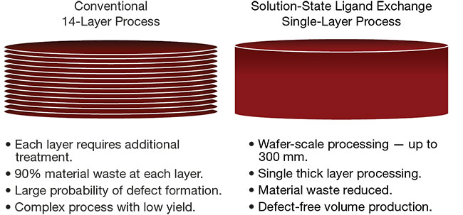
Fabrication of conventional quantum dot sensors involves a multilayer deposition process that carries risks of defect formation (left).
New ink technology allows deposition of a single layer of nanoparticles, which saves both time and materials while improving yields (right). Courtesy of Quantum Science Ltd.
Several CQD synthesis and device manufacturers have faced significant challenges related to the control of nanoparticle synthesis and quantum dot degradation upon exposure to air and moisture, the poor performance of the resulting photodetectors, and operational stability.
Maintaining batch-to-batch consistency is one of the major challenges for CQD suppliers, who must control each stage in the multistep manufacturing process. Inadequate process control results in known issues such as poor uniformity of nanocrystal size, shape, and elemental composition; improper chemical binding of a quantum dot’s surface; and impurities and organic content in the colloidal system. Improving process control requires expertise in quantum dot synthesis and scale-up, surface chemistry, ink formulation, and fabrication and testing of the nanomaterials in optoelectronic devices.
In the wet chemistry process typically used to make CQDs, long-chain organic ligands are commonly used to control the growth of the nanocrystals and maintain their colloidal stability in solvents.
For optoelectronic devices, the long-chain insulating organic ligands are
replaced with shorter and more conductive ligands to increase electronic coupling among the nanoparticles in solid films. The ligand exchange processes are typically carried out on solid-state nanoparticles or in solution.

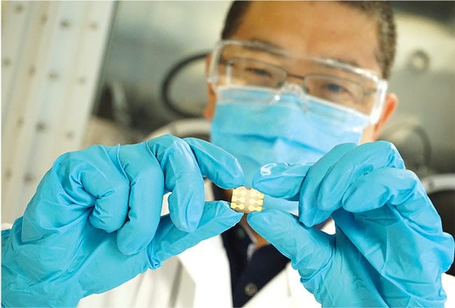
Quantum Science Ltd. fabricates dots using benchtop wet chemistry that employs a ligand exchange process in solution to ensure optimal optoelectrical performance. Courtesy of Quantum Science Ltd.
State-of-the-art CQD devices use solid ligand exchange, requiring multilayer deposition of a thin CQD film. Each layer requires additional chemical treatment and washing steps to replace the insulating ligands on the dots’ surface. This repeating layer-by-layer process is time-consuming and inefficient — and generates a high probability of defect formation and low yield.
A new ink technology reduces some of these problems. Available for lead-based and lead-free quantum dots, the inks potentially overcome several hurdles that device-makers confront by replacing solid-state, multilayer deposition techniques with a solution that can deposit a CQD coating in a single step. The simplified process saves time and money and opens up the possibility for mass-market-scale production of high-performance
optoelectronic devices. The ink technology also enables the fabrication of
optoelectronic devices on diverse substrates and form factors by using solution-processing techniques such as spin or spray coating; continuous roll-to-roll, blade, or slot-die coating; and inkjet
printing.
Tunability means versatility
Single-step coating facilitates CQD processes for a range of form factors, such as CMOS wafers, glass, and flexible thin-film transistors. As a cost-effective and high-performance solution with tunable sensitivity, SWIR CQD technology
unlocks significant future market opportunities for a wide range of applications that require detection of wavelengths
between 1.3 and 2.1 µm, such as under-display facial recognition for smartphones, more eye-safe VR headsets, reduced-cost sensing for advanced driver assistance systems, and industrial automation systems.
The technology expands sensor solutions within the SWIR range. For instance, SWIR wavelengths from 1.45 to 1.9 µm are highly absorbed by water. As a result, images of objects with high water content — such as bruised fruit, irrigated crops, liquid mixtures, and black ice on roads — appear black when illuminated with these wavelengths. In addition, SWIR imagers can clearly distinguish among certain plastics, chemical compounds, and skin conditions.
In addition to the tunable absorption wavelength of quantum dots, the technology’s detection limits extend beyond conventional SWIR detector InGaAs or SiGe to offer sensor developers a versatile new platform for design. Further, the
suspension of quantum dots in advanced ink technology greatly simplifies their deposition to offer streamlined, cost-effective, scalable sensor manufacturing processes able to meet demand in an expanding list of applications.
Meet the authors
Cong-Duan Vo, Ph.D., is CTO at Quantum
Science Ltd. He has more than 20 years of R&D experience in material synthesis,
surface chemistry, quantum dot resin, and
ink formulations and films; email: [email protected].
Stuart Stubbs, Ph.D., is product director at Quantum Science Ltd. He has over 10 years of experience in managing optoelectronic devices from proof of concept to commercialization. Stubbs holds 25 patents in quantum dot
materials and processes and optoelectronic devices; email: [email protected].
Hao Pang, Ph.D., is the founder and CEO of Quantum Science Ltd. He holds a doctorate in materials chemistry from the University of Strathclyde and an MBA from the Manchester Business School. Pang has nearly two decades of materials research and commercialization experience; email: [email protected].
Acknowledgments
The authors thank the Quantum Science
technical and product teams and collaborators for their dedication and teamwork on material innovation, scale-up, and product development.
References
1. S. Manda et al. (2019). High-definition visible-SWIR InGaAs image sensor using Cu-Cu bonding of III-V to silicon wafer. 2019 International Electron Devices Meeting (IEDM), pp. 16.7.1-16.7.4.
2. A. Clouet and E. Mounier (2022). SWIR
Imaging 2022: Market and Technology Trends. Yole Développement.