For semiconductors, smaller is better.
That’s why the industry may soon take a big step down. On the horizon is a
switch from 193- to 13.5-nm-wavelength lithography. This extreme-ultraviolet (EUV)
technology eventually could allow an almost tenfold shrinking of current chip features.
The surest sign that EUV is about to be deployed after years of
development is money, said Stefan Wurm. He is associate director of lithography
at the Albany, N.Y., branch of Sematech, the Austin, Texas-headquartered semiconductor
research consortium.
In July 2009, leading lithography toolmaker ASML Netherlands BV
of Veldhoven announced the availability of EUV scanners for process development.
That milestone has been followed by another.
“As of late February this year, six companies have committed
to buy such tools. That’s really significant,” Wurm said. “Each
of those companies – to buy one of those tools, install it and get it running
– is probably looking at an investment that exceeds $100 million.”
But to paraphrase Mark Twain, rumors of the imminent death of
193-nm lithography have been greatly exaggerated. It – and even longer wavelengths
– will be around for years.
Repeating history
In the past, semiconductor makers have moved down in lithography
wavelength, when necessary, to pattern finer features. For example, before 193-nm
lithography, which is powered by ArF lasers, the industry used KrF lasers at 248
nm. Thus, some argue, EUV is really in keeping with tradition.
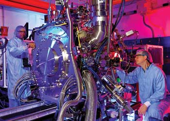
This lithography source for extreme semiconductor manufacturing uses a laser-induced
plasma to produce extreme-ultraviolet, or 13.5-nm, photons, which will be used to
pattern future semiconductor chips. Courtesy of Cymer Inc.
“What we’re doing is nothing different than what we’ve
done before. It’s just a factor of 14 instead of a factor of 1.5,” said
Vivek Bakshi, president of EUV Litho Inc., also of Austin. The company promotes
its namesake through consulting, workshops and education.
In some ways, the new lithography and its deployment are really
business as usual. Bakshi noted that many of the current lithography modeling tools
and techniques still apply because EUV still projects photons to print a pattern.
The switch does demand some changes from current practice, however.
EUV lithography must be done in a vacuum because the photons are absorbed by air.
Routing the light around and focusing it on the wafer must be done via reflection,
not refraction. Thus, mirrors are required, and the masks must be reflective, not
transmissive.
Scalable sources
EUV also requires a completely new yet cost-effective and reliable
source. Versions have been demonstrated that hit 100-W output power, enough for
minimal production. High-volume manufacturing will require doubling that figure.
The EUV source from Cymer Inc. of San Diego uses a high-powered
infrared laser to bombard a microscopic molten tin droplet as much as 50,000 times
per second. The resulting plasma radiates photons over a range of wavelengths. The
13.5-nm light is collected and directed into the scanner illuminator.
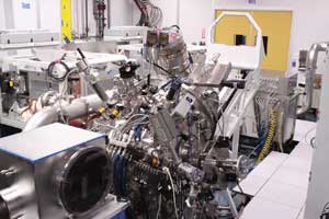
Because 13.5-nm photons are absorbed by air, and lenses that focus them are lacking, sources
for extreme-ultraviolet lithography must operate in a vacuum and route light using
mirrors. Courtesy of Cymer Inc.
Cymer is a leading supplier of deep-ultraviolet light sources.
For EUV, the company went with a laser-produced plasma rather than generating one
between electrodes because of some fundamental advantages.
“It’s a scalable power solution. The plasma is in
space. It’s not close to any of the hardware,” said Nigel Farrar, Cymer’s
vice president of global lithography applications and technical and strategic marketing.
Besides keeping the plasma at a distance and minimizing damage
from it, this scheme also allows for collecting photons over a wider angle. A downside
is that it required development of a suitable laser. Further advances in source
power could come from the laser as well as in more efficient conversion of its pulses
into EUV photons.
Cymer is supplying the sources for ASML’s prototype production
EUV scanners. Farrar said that the source deliveries are on track.
Gigaphoton Inc. of Oyama, Japan, also is pursuing a laser-based
approach. The company has announced plans to start shipping EUV light sources next
year.
Mirror, mirror on the scanner
Carl Zeiss SMT AG of Oberkochen, Germany, makes another key lithography
component for ASML’s scanner. Zeiss supplies the projection optics, a set
of six mirrors that bounce the light from the mask onto the wafer. The mirrors must
be polished precisely, with a roughness of about 100 pm across more than 300 mm.
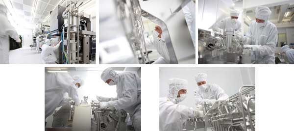
ASML technicians assemble the first preproduction extreme-ultraviolet patterning scanner in a cleanroom in Veldhoven, the Netherlands. Courtesy of ASML BV.
Over that span, the reflectivity, which is about 70 percent, can
vary only in the hundredths of a percent at the central wavelength. What’s
more, the mirror pointing and positioning are exacting, with the latter tolerance
better than 1 µm.
Winfried Kaiser, senior vice president for product strategy at
Carl Zeiss SMT, noted that the tug of the earth cannot be neglected. “Gravity
can introduce aberrations. So the art is to hold this heavy mirror without deformation.”
ASML director of corporate communications Lucas van Grinsven said
that the company has commitments from six customers for its EUV scanners. The six
potential buyers are scattered over all parts of the world and represent all segments
of the semiconductor industry.
The first of the preproduction systems is slated to ship this
year. In mid-June, van Grinsven said: “Just last week, we’ve integrated
the first complete system. So that all looks beautifully on track.”
By 2012, he continued, ASML must be able to provide production
systems that could then be churning out chips in volume a few years later. The likely
insertion point, he said, will be around the 20-nm half-pitch or smaller memory
technology node, which will have considerably finer features than today’s
45- and 32-nm nodes.
In its new scanners, ASML is trying to change only what it must.
The company, for example, is employing the same wafer movement mechanism in the
new tools that it does in the current ones.
Inspecting masks and other hurdles
This march to EUV does face some significant hurdles. Making masks
of sufficiently high quality, for instance, is still a challenge. Another is checking
for defects in those masks initially and after use.
Brian Trafas is chief marketing officer for KLA-Tencor Corp. of
Milpitas, Calif. The company makes mask inspection tools, including one capable
of handling 22-nm logic node EUV masks. The tool does this using a 193-nm source,
but Trafas said that this would not work for the 16-nm-and-smaller nodes.
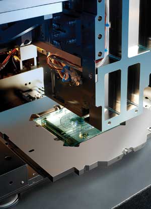
To make working chips, you need defect-free
– or defect-free enough – masks. As chip features get smaller, verifying
that becomes harder to do. A new reticle defect inspection platform from KLA-Tencor
Corp. does this for 2x-nm, such as 22-nm, lithography through innovations in imaging
and computational lithography. Courtesy of KLA-Tencor Corp.
“We need to inspect the EUV masks at the same basic wavelength.
So today we’re OK, but as we look toward the future, we believe actinic is
necessary for success,” he said.
Developing such a capability will not be cheap. The new tool,
for instance, will need its own EUV source and associated vacuum-based materials
handling. To help defray that cost, KLA-Tencor is seeking outside funding from other
industry players.
Carl Zeiss SMT likewise makes an inspection tool, said the company’s
Kaiser. The company also is looking into building an inspection tool with an EUV
source.
A double take on alternatives
There is the chance that EUV will prove to be too expensive. There
are alternatives to it, such as extensions to current technology.
However, 193-nm lithography can print only 22-nm half-pitch features
through double patterning. As the name implies, this puts product through lithography
twice. Further shrinks could necessitate double-double patterning. Because it requires
only a single pass, EUV has cost and space advantages.
In this decision about when to deploy the new lithography, it
helps that EUV need be employed only initially on the most demanding layers. What’s
more, some of the earliest uses of EUV probably will be to pattern dense contact
hole layers.
That mitigates against the need to produce masks of the lowest
defect level, Sematech’s Wurm said. “You don’t have a large open
area, so defects don’t matter that much.”
Finally, in the semiconductor industry, keeping up with the Joneses,
innovation-wise, is a requirement. Thus, the industry may hesitate while alternatives
are evaluated but then move quickly to embrace a solution. If companies do otherwise,
they risk missing a competitive advantage. That may be the case with the new lithography.
As EUV Litho’s Bakshi said, “Nobody wants to be left
behind in this industry. You don’t get a second chance.”