Digital optics manufacturing approaches have led to advancements that are shaping the future of high-tech devices in illumination and imaging applications.
Marco de Visser, Lumenworkx Engineering
Optical components have traditionally been created through subtractive manufacturing approaches that are mainly based on turning and molding methods. Milling, for example, is an affordable way to rapidly develop a first rough prototype. Milling is generally considered to be a low-end optics fabrication solution, but it is suitable for routine form and fit testing of components. More accurate, though expensive, diamond-turning techniques are used for high-end optical solutions. In this method, once the functionality of the optics design and the physical part performance are validated, soft tooling can be adopted, or, if quantities allow, a direct investment in hard tool fabrication can be made to enable volume manufacture through injection molding.
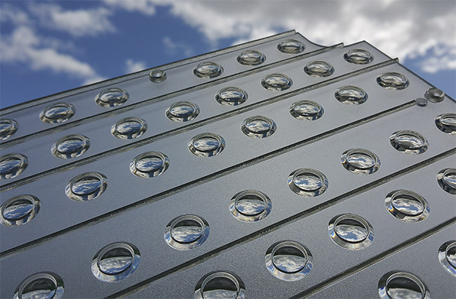
A large-format lens array with both optically smooth and frosted finishes. Courtesy of Luximprint.
But new technologies enabled by additive approaches are changing the game when it comes to the speed, flexibility, and cost-efficiency of manufacturing optics. Additive processes eliminate some of the production complexity of traditional manufacturing, while at the same time opening doors to new opportunities in design and materials. This will benefit a wide range of industries, including automotive, aerospace, and medical.
The tooling required for conventional optics manufacturing methods comes at a price. This price includes time-to-market delays (caused by the long tooling lead times for customized solutions), significant upfront investments, and minimum order quantity requirements to ensure mold amortization and proper parts prices, which, in turn, may lead to large inventories and costly inventory write-offs. From a multidisciplinary perspective, tooling has been a proverbial thorn in the side of those involved in the design, development, manufacturing, and marketing processes of optical components.
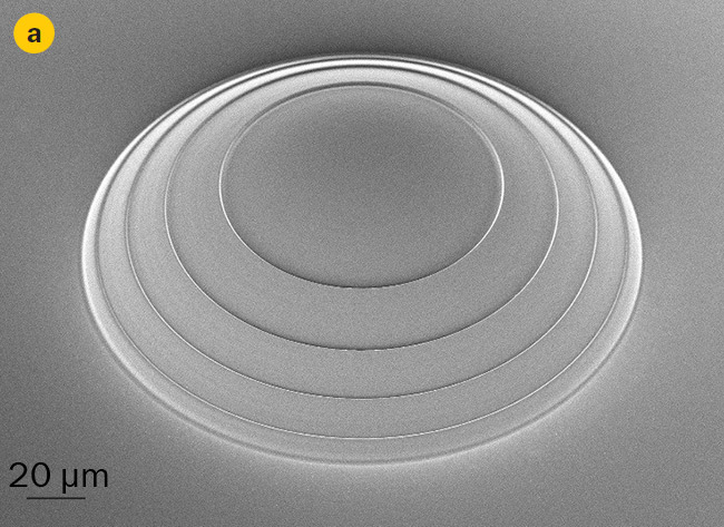
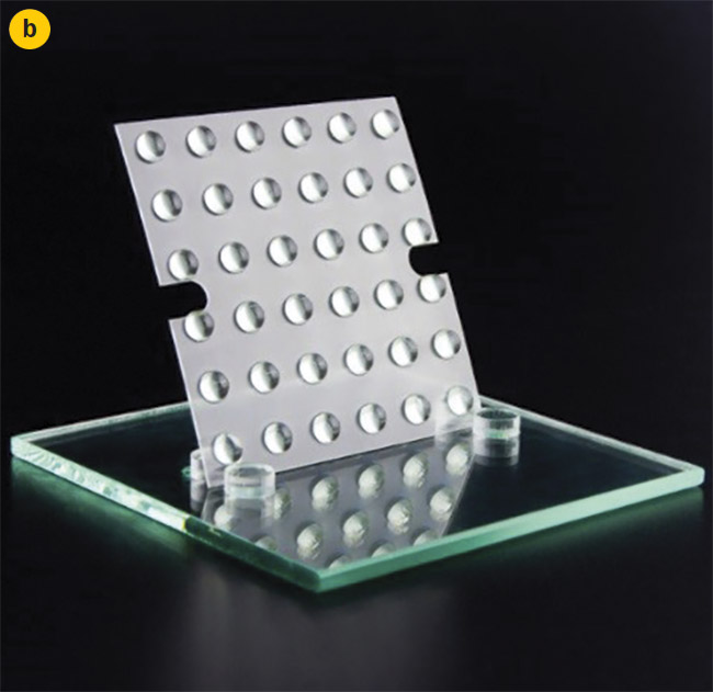
Two-photon grayscale lithography enables the fabrication of a combination of refractive and diffractive elements in micro-optics in one production step (a). Single lenses with spherical, aspherical, and freeform shapes (b). Courtesy of Nanoscribe.
21st-century optics
About a decade ago, the first digital optics fabrication technologies were implemented for regular use. Inspired by the increasing application of 3D-printing technologies and motivated by the limitations and costs associated with conventional methods, several industry leaders (many from smaller firms) began to reinvent the manufacturing of optics using an additive approach. Hence, a variety of successive optics production techniques were born, each aiming to bridge the gap between digital design methodologies and the ever-increasing market need for more diversification. As manufacturing evolved, so did new possibilities in both design and assembly. The Third Industrial Revolution for optics took shape.
In sharp contrast to conventional subtractive approaches in which material is removed, 3D printing adds successive layers of optical resins. A variety of jetting and layering methods is used, whereby liquid resins get cured into solid objects through light or thermal curing. The most common techniques for additive optics include UV inkjet printing, direct laser writing, and stereolithography.
Benefits of additive optics
Before detailing each additive optics method, an explanation of the advantages of 3D-printing optics is warranted.
Manufacturing speed. The majority of the available additive optics processes operate at very high speeds. Direct digital manufacture of optics, or one-step “CAD-to-optic” fabrication, avoids the limitations of typical tooling and molding processes, and lead times for custom optics drop from months to weeks or even days. As a result of the increase in production speed, the costs also drop.
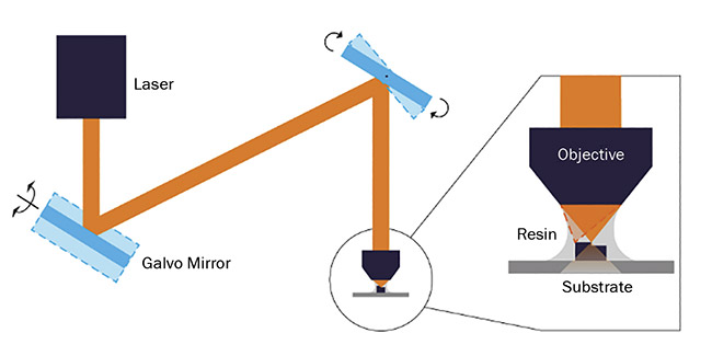
A schematic of a two-photon polymerization (2PP) setup. 3D printers that utilize 2PP enable highly precise and fast fabrication of micro-optics. Courtesy of Nanoscribe.
Toolless fabrication. In additive optics methods, the mold is digital, with only the CAD file needed to fully describe the optical characteristics and to start the fabrication. Optics can be printed on demand — to demand — with no minimum order quantity requirements. In fact, the minimum order quantity is theoretically just one. As a result, physical stock levels decrease, and working capital is available for alternative use and innovation. Optical stock has become a digital asset.
Increased flexibility. The flexibility of additive manufacturing is evident in both the manufacturing process itself and in the upfront design process. Whereas a traditional manufacturing job contains only one design at a time, a combination of jobs and multiple designs is now possible with additive methods, as long as the lens type, setting definitions, and design characterizations allow it. This latitude encourages designers and engineers to build variations into a their products, or to optimize (iterate) the design once errors are exposed after the first prototypes are tested.
Free complexity. Within the ever-
expanding boundaries of what is printable, there is no penalty for complexity in the additive optics process. Costs for a traditional complex mold can be prohibitive, but the complexity of a CAD file has minimal impact on the printing process. Fabrication of complex optical shapes and textures has become as easy and cost-effective as much less-complicated concepts.
Additive optics methods
The current landscape of the additive fabrication of optics is well-balanced, augmented by the integration of complementary technologies. Each of the following approaches covers a distinct field of application or research, or multimarket scope.
3D microfabrication. The two-photon polymerization (2PP) maskless lithography technique is used for 2D and 2.5D digital micromanufacturing of highly precise optical components for nano- and microscale structures. This process produces ultrasmooth micro-optics with excellent shape accuracy in just one fabrication step, enabling enormous design freedom. Lateral feature sizes are typically scalable down to 160 nm.
The 2PP process is compatible with a broad range of print materials and substrates, including glass. With a typical build volume of 100 × 100 × 8 mm³, and a typical layer thickness of 0.3 to 5 μm (values depend on the objective and photoresin used), a surface quality of ≤20 nm (Ra) can be achieved. This precision makes the process well suited for research and rapid prototyping of components in microfluidics, photonic metamaterials, micro-optics, and nanostructures.
Two-photon grayscale lithography (2GL) systems are designed for the microfabrication of prototypes and masters in industrial production processes. This technology combines the performance of grayscale lithography with the precision and flexibility of 2PP. This maskless lithography system upgrades the fabrication of freeform micro-optics, microlens arrays, and multilevel diffractive optical elements. New printing materials for creating high-refractive-index micro-optics with special properties are available, and specific photoresins feature a high refractive index in combination with high dispersion, which corresponds to a low Abbe number.
Challenges remain with these additive manufacturing microfabrication approaches, such as the ability to create larger optical components. In addition, the high-precision-writing mode of these methods causes the writing speed to be relatively slow compared to other high-speed optical 3D-printing processes. This limits the extent to which these techniques can be scaled up to industrial volume manufacturing. Also, a correspondingly high experimental effort and significant financial resources are necessary to make these processes viable. Despite these challenges, this technology is in a unique position to generate high-end prototypes and production masters for use in experimental research and advanced industrial environments.
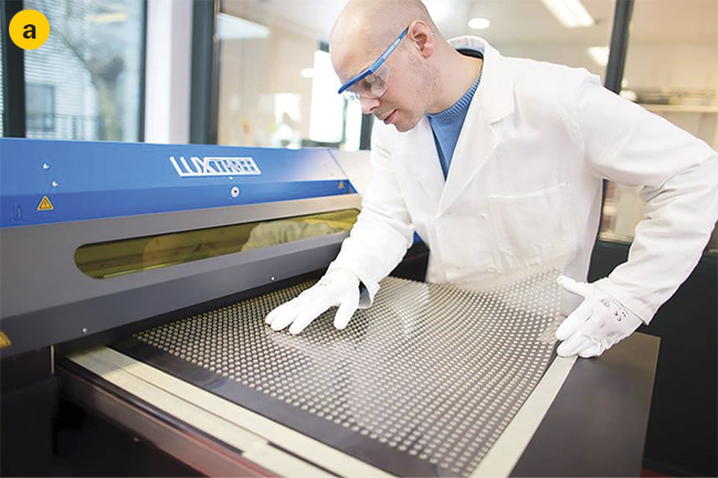
Printoptical technology is used to create flexible (a) or rigid (b) large-format optics. Courtesy of Luximprint.
CAD-to-optic manufacture. Whereas the 2PP process involves the 3D-printing of nano- and millimeter-size objects, Printoptical technology 3D-prints larger macro-optical structures using proprietary advanced wide-format industrial inkjet equipment. Typically engineered for high-volume printing, droplets of a transparent UV-curable polymer resin are jetted onto a translucent substrate and then cured by UV lamps that are attached to the print heads. The picoliter-size droplets are deposited in several passes until the desired form is built.
The resulting optical surfaces are smooth and perform functionally as is, or they can also be given a frosted finish. The smoothness is accomplished by allowing time for the droplets to flow and merge into the desired shape before curing, taking advantage of the effects of surface tension. Optical-quality surfaces can thus be achieved with no further processing.
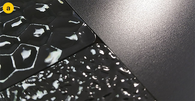

Custom textures are available for large-format optics: aluminum-coated textured surfaces (a) and macrolens arrays (b). Courtesy of Luximprint.
A sheet of acrylic is used as a carrier for the printed optical features. Polyethylene terephthalate (PET) films, polycarbonate sheets, or even glass substrates can be used as well, along with a broad range of pre-manufactured lens parts and substrate materials. Build thicknesses range from 0.3 to 10 mm, with a variety of sheet thicknesses possible. The design of the equipment allows a printed optic to be made in any size, up to the total available print area of 600 × 1000 mm. After printing, the substrate can be left as a single optic or can be cut into smaller arrays or individual lenses.
CAD-to-optic manufacturing can create geometric or freeform lens shapes, frosted finishes (VDI-like textures), light guide plates, micro-optics, fully opaque surface masks, and colored and textured adjacent surfaces (Optographix) that can be integrated into a part of a printed optic. Typically, large-format optics solutions are involved.
Hybrid additive optics. Direct CAD-to-optic methodologies can expose limitations in the resins used, most notably in lifespan, temperature resistance, and build volume. As an alternative, a hybrid smart optics manufacturing approach aims to overcome these obstacles to produce custom lenses while further expanding the overall design freedom and three-dimensional build volume.
This method leverages the speed of 3D printing and combines it with proven casting technologies to generate a custom optical design. This technique can produce intricate optical designs with ease, eliminating cost-saving compromises.
After printing a master part using this method, its counter negative — a smart tool — is created, taking full advantage of the optically smooth surfaces of the core 3D printing process. As a next and final step, the optic is cast in a crystal-clear, durable optical polyurethane material.
Smart manufacturing of optics enables scale
prototyping and pre-series production with
affordable, industrial-quality optics. Courtesy
of AddOptics.
Whereas direct CAD-to-optic manufacturing offers limited manufacturing freedom due to a lack of support materials and sheet integration, smart manufacturing of optics offers much more freedom. Optical parts are easily generated in higher volumes, and, if required, multiple runs can be combined. This method enables scale prototyping and production of affordable, industrial-quality optics.
The process offers an average shape accuracy of less than 40 µm and surface qualities up to 15-nm rms and beyond. Lenses and light guides made via this method — including total internal reflection collimator lenses, aspherical lenses, freeform surfaces, and Fresnel lenses — are used in illumination and entry-level imaging systems.
Printed glass optics
The ability to 3D-print glass is essential for developing the highly complex, freeform, and small-scale optical structures needed to enable next-generation photonics, sensing, and imaging technologies. Yet it has proved difficult to 3D-print glass, which has a high melting point of over 1400 °C. Retaining glass’s unique chemical, mechanical, and optical properties throughout the additive process is critical to success.
New techniques for 3D-printing transparent glass are under development. While most of these approaches are still in their infancy at the research level, the first commercially available methods are beginning to see the light. Also, promising research is underway that involves the use of direct laser writing and stereolithography to print the nanoglass particles included in polymer pastes.
Direct laser writing technologies have evolved as a 3D-printing method capable of fabricating 3D micro-optics with submicrometer feature sizes and optically smooth surfaces. For printing glass, this process uses a two-photon curable silica nanocomposite resin that can be structured so that the printout is convertible to transparent fused silica glass via thermal debinding and sintering.
After a final heat treatment, the polymeric nanocomposites are turned into high-quality fused silica glass. The conversion takes place at 700 °C below the temperature at which silica melts (approximately 2000 °C). The sintered parts are chemically and physically indistinguishable from commercial fused silica glass. They show the same high optical transparency in the UV (84% at 200 nm), visible (>92% at 200 to 1000 nm), and infrared (>90% at 1000 to 3400 nm) regions of the light spectrum.
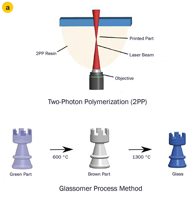
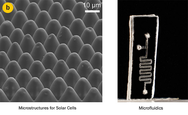
A schematic of a printed glass optics process method (a). Printed glass
microstructures for heat-critical
applications such as solar panels and microfluidics (b). Courtesy of KIT/
NeptunLab, Glassomer, Nanoscribe.
Fused silica is the material of choice for many high-performance components in glass optics due to its high optical transparency combined with its high thermal, chemical, and mechanical stability. Generating fused silica microstructures for micro-optics, embedded structures, and microfluidics is of high interest to the optics industry. It will enable a wide range of next-generation complex-shaped optics and photonics applications with resolutions on the scale of tens of micrometers and surface roughness of 6 nm (Ra).
Outlook
The last decade has brought several additive optics approaches to be further fine-tuned. Recent advancements have resulted not only in successful implementation of additively fabricated optical plastics, but also in breakthroughs in 3D-printed glass optics. While not all of the technologies are commercially viable yet, they continue to develop at a significant pace.
From micro- to macroscale optics and from plastics to glass, today’s optics industry is changing. Additive methodologies are overcoming the disadvantages of subtractive fabrication techniques, opening up doors to greater freedom in design, materials, and applications for a wide range of industries. A “cross-
pollination” of conventional and futuristic approaches will lead to a better product.
Meet the author
Marco de Visser is the founder of Lumenworkx Engineering and the co-founder of Luximprint. He has over a decade of experience in the field, working with combined lighting, optics, and 3D-printing technologies. He advocates for the development and adoption of novel additive fabrication methods and other new technologies for startups, scale-ups, and industry leaders in search of inventive solutions for everyday challenges.