As imaging plunges into the depths of the UV spectrum, component-makers mix advancements from commercial products with modified materials to meet the challenges of working in the UV.
MARIE FREEBODY, CONTRIBUTING EDITOR
Feature sizes of modern electronics continue to shrink, approaching or even surpassing the wavelength of light, and equipment manufacturers are looking for new ways to improve the optical resolution of their systems to inspect ever smaller structures.
One way to do this is by reducing the wavelength of the illumination. While in the past this has moved the light source
to the blue end of the visible spectrum, some applications are shifting into the near UV, the deep UV (DUV), or even the extreme UV (EUV).
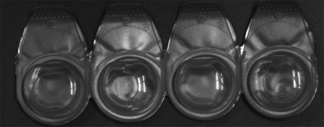
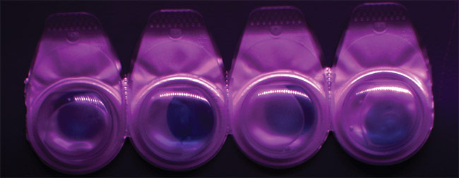
Under visible light, clear contact lenses appear
clear in their packaging, creating minimal or no
contrast to verify their presence (top). The use of
UV light at 365 nm and a bandpass filter creates
enough contrast to verify lens presence (bottom).
The contact lenses have a UV-blocker coating,
so they block the UV light and appear darker.
If a lens was missing or lacked a UV coating, it
would appear brighter, similar to the backlight,
rather than darker. Courtesy of Midwest Optical Systems.
Imaging in the visible and near-infrared (NIR) has established applications in both machine vision and security applications. UV imaging is fundamentally the same as visible imaging and similar to NIR imaging, but with one crucial and problematic difference: energy.
Shorter wavelengths carry more energy. Higher-energy illumination sources and detectors have a shorter lifespan compared to visible and NIR components. Furthermore, component efficiency is lower and component cost is higher, detrimentally affecting system economics.
“As you move farther from the visible electromagnetic spectrum, other factors
become important — for example, material transparency, optical properties, and damage mechanisms due to energy density,” said Dale Deering, senior director of business development for Teledyne DALSA. “This increases the challenge of using UV as the wavelengths get shorter.”
The use of high-energy UV light, especially in UVB and UVC regions, poses a risk — in the form of eye damage and skin irritation (think sunburn) — to nearby humans, even with only momentary or brief exposure. Many of these lamp and light sources are regulated under IEC 62471 and classified into risk groups. Deploying these systems requires taking extra safety precautions, such as enclosing systems to prevent unintentional light exposure.
But the news is not all bad. Today’s light sources, cameras, sensors, and lens components are engineered for UV applications and show promise in minimizing
damage. These improvements should boost the use of UV imaging in machine vision and beyond.
Turning down the heat on UV
UV imaging in machine vision became practical with the commercialization of UV LEDs, which have since undergone significant generational upgrades.
Years of research have led to improved UV emitter efficiency — boosted in large part due to substantial improvements in substrate quality — which has pushed internal quantum efficiency above 80% across a wide wavelength range.
However, both the carrier conversion efficiency (external quantum efficiency, or EQE) and power conversion efficiency (wall-plug efficiency, or WPE) of UV LEDs remain significantly lower compared to InGaN-based blue LEDs. These factors, along with cost considerations, have hindered widespread adoption, but niche applications abound.
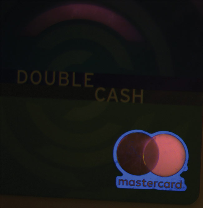
Without the use of a filter, the background of a credit card can confuse an imaging system that is trying to verify a certain area or feature, in this case the logo at the lower right. Courtesy of Midwest Optical Systems.

Matching a precise bandpass filter to the fluorescence band of the logo eliminates the background and image noise. This improves repeatability and image processing speed. Courtesy of Midwest Optical Systems.
“Though they’re not as bright or
efficient as their visible counterparts,
UV LEDs have reached a point where
we can make lights bright enough to be suitable for imaging without excessive heat or the need for active cooling,” said Steve Kinney, director of training, compliance, and technical solutions at Smart Vision Lights.
The emergence of monochromatic UV lasers and LEDs is particularly useful in machine vision applications. Pairing
single-wavelength UV sources with appropriate bandpass filters eliminates the need for achromatic camera optics, significantly lowering cost.
“UV imaging has changed in both the lab and on the factory floor,” said James Gardiner, business development manager at Midwest Optical Systems Inc.
(MidOpt). “Higher-power and higher-efficiency UV light sources such as
LEDs and laser diodes help us create more fluorescence or spectra signals.
This has been critical in the success of imaging materials that would otherwise have low signal return when exposed to UV lighting.”
Most of today’s UV imaging systems function between 350 and 400 nm. The high energy of shorter wavelengths can degrade the materials they illuminate, even with short exposure times.
“At around 250-nm wavelength, the
energy of the photon becomes large enough that it can actually damage the silicon surface of silicon semiconductors
used in imagers and ICs [integrated
circuits] for electronics,” Kinney said.
UV cameras: cost and resolution
Modern image sensors are predominantly made from silicon, which UV light does not penetrate well, with wavelengths shorter than 350 nm absorbing at depths of less than 1 µm. Illuminating a charge-coupled device (CCD) or complementary metal oxide semiconductor (CMOS) image sensor solely from the front results in poor detection or imaging performance even for visible-light applications. The problem is worse for UV because of its poor penetration depth in silicon.
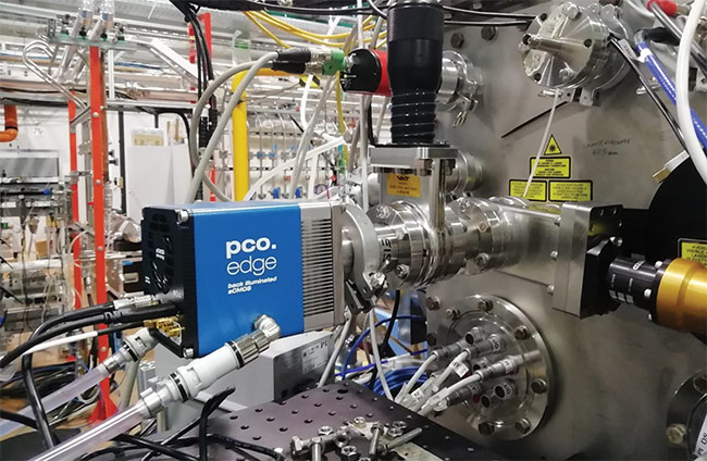
The Excelitas pco.edge 4.2 bi XU, a camera that is sensitive in the extreme UV and soft x-ray ranges, is connected to a synchrotron at Elettra Sincrotrone Trieste in Italy. The camera is an example of technology that has traditionally been used in research, but it is also suited to the increasingly challenging requirements of quality control in front-end semiconductor testing. Courtesy of Excelitas PCO GmbH.
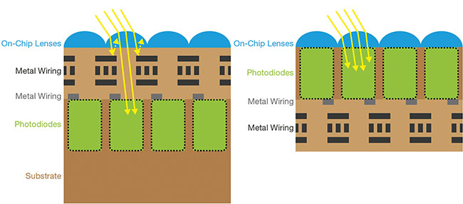
A schematic cross section of a front-illuminated CMOS image sensor with microlenses (left) and a back-illuminated CMOS image sensor with microlenses (right), illustrating the differences of each in penetration depth and performance. Courtesy of Excelitas PCO GmbH.
Fabrication advancements enabled economical wafer-scale manufacturing of back-illuminated image sensors that improve penetration depth by thinning the silicon layer. To make these sensors, all of the layers are deposited and then the wafer is turned and the substrate material etched or thinned, and the image sensor is illuminated from the back side. The technology has been widely used to improve low-light visible imaging, but the approach is even more important for UV applications in which penetration depth
is so poor.
“Now the penetration depth of the UV light is enough to generate charge carriers in the silicon, opening quantum efficiencies/sensitivities down to 193 nm and lower,” said Gerhard Holst, senior imaging product and applications scientist at Excelitas PCO GmbH in Kelheim,
Germany. “With a proper coating and
material, it is also possible to create
image sensors that are sensitive down
to 2 nm, which means extreme UV and soft x-ray.”
Silicon is far from the only optical
material that is problematic for UV.
Standard optical glass absorbs light in the
region below 290 nm. To sidestep this problem, early UV cameras relied on visible imagers, but with the blocking elements removed. Modern cameras use optical components of fused silica, fused quartz, and/or calcium fluoride, which allow more of the desirable UV light to pass through.
Below 180 to 190 nm, air also becomes an issue for UV imaging because it absorbs the light. This portion of the UV spectrum, often referred to as the vacuum UV (VUV), requires a very high vacuum or nitrogen environment.
Inevitably, alternative materials and additional manufacturing steps deliver performance at a cost. Nick Sischka, director of imaging product development at Edmund Optics, said UV-specific cameras can cost up to an order of magnitude, or 10×, more than visible light cameras at a comparable resolution.
On the upside, as CMOS has become more prevalent in imaging, consumer-driven improvements to CMOS imagers have also improved their UV response and widened their blue response further into the UV range.
“Certainly, UV cameras using standard visible CMOS imagers with the blocking
elements removed are much better today than in the early days,” Kinney said. “However, some camera manufacturers have taken this even further. There are now UV-specific imagers where the
photosensitive depletion layer in the
pixel is specifically designed and tuned for UV performance.”
For example, the MV4-D1280U-H01-GT UV camera from Photonfocus AG
features a back-thinned CMOS imager that achieves a quantum efficiency response of more than 30% at 175 nm, on par with the performance of standard visible imaging.
But for OEMs, the exotic thinning process limits yield and raises costs.
To facilitate UV-sensitive camera
development, the Sony IMX487 delivers
a UV-wavelength-compatible sensor suitable for OEM camera integration. The simplicity makes it attractive for OEMs to design UV cameras for applications in the semiconductor industry, plastics sorting, infrastructure inspection, coating detection, and more.
Still, UV image sensor resolution is in the range of 4 MP, which is not particularly high by modern imaging standards. Holst said he expects that this resolution will increase, with smaller pixel sizes that can operate at lower magnifications.
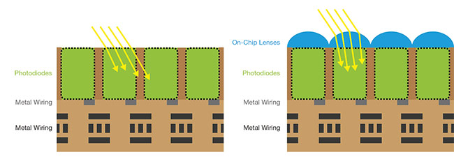
A schematic cross section of a back-illuminated CMOS image sensor without microlenses (left) and with microlenses (right), illustrating the effects of each option on the modulation transfer function. Courtesy of Excelitas PCO GmbH.
“I guess it can be expected that the semiconductor industry will further increase the integration level of transistors per area, and therefore the actual illumination wavelength of 193 nm might become even lower,” Holst said. “Image
sensor solutions will be [ready to meet the requirements], but the demand on the lens material will be greater.”
Cellphone market boosts UV optics
Few optical materials are suitable for UV use, largely due to the high level of absorption and dispersion present in most materials in the UV. The best UV optics are expensive and made from materials that have better transmission of the short UV wavelengths — such as calcium
carbonate, quartz, or other exotic materials — than is offered by standard glass.
‘Now the penetration depth of the UV light
is enough to generate charge carriers in the silicon, opening quantum efficiencies/sensitivities down
to 193 nm and lower.’
— Gerhard Holst, senior imaging product and
applications scientist at Excelitas
The material’s grain quality and size have become the decisive features for UV optics. In an unexpected but welcome offshoot of the drive for better cameras
in cellphone and consumer imagers, grain size has been at the forefront of research.
Cellphone and consumer imaging markets have driven the development of imagers of over 10 MP, which means that the size of an average pixel on common imagers has steadily shrunk. This market drive to smaller pixels has in turn led to an abundance of lenses made with better glass and the ultrafine grain size needed to support sharp resolution, inadvertently expanding the suite of optics available for UV imaging.
“While UV users still have to choose better-than-average-quality glass lenses, there are now many standard choices that can support UV imaging down to around 350 nm,” Kinney said. “Users needing
to image below 350 nm still have to rely on the more exotic lens materials though.”
Getting to the fine detail of UV inspection
The semiconductor industry is the largest market for UV imaging. In the continuing quest for smaller semiconductors, UV imagers must resolve ever finer structures
on semiconductor masks for wafer production, quality testing, and detecting or measuring detrimental particles. As a result, illumination wavelengths for semiconductor image analysis have dropped from 254 to 193 nm in recent years, Excelitas’ Holst said.
UV also plays a role in inspecting optically clear plastic, glass, coatings, and adhesives. In essence, UV imaging is employed wherever it enables the user to take advantage of the material properties of the object being imaged.
For example, grease tends to fluoresce in UV light, which simplifies the task of determining how much grease lies within ball bearings and other movable joints.
“Due to the dark nature of grease and the narrow places it is commonly applied, [seeing grease] was previously difficult using standard monochrome or color imaging,” Kinney said. “This kind of detection technique applies to many glues, epoxies, and silicone adhesives used in parts assembly.”
In another example, Sischka noted that contact lenses are highly absorptive in the UV range. This means UV light can be used to highlight the contrast between a transparent contact lens and other clear surroundings that would otherwise be hard to differentiate using conventional visible imaging techniques.
“Under visible light, a clear contact lens appears clear in its packaging.
This creates little to no contrast of the contact lens and the packaging,” Sischka said. “By using a UV light and a UV
365-nm bandpass filter, we can create contrast between the contact lens and
the packaging.”
Other applications include plastic or glass waste sorting, electric power plant inspection, watermark identification in bank notes, fine scratch inspection, multispectral imaging, and maintenance of electric power cables.
“It has become more common to see companies incorporate UV tracers into visibly clear adhesives and coatings to make them fluoresce when exposed to UV,” MidOpt’s Gardiner said. “This fluorescence has allowed machine vision systems to inspect for voids, breaks, or defects when these visibly clear adhesives and coatings are applied.”
Agricultural imaging, both in the field and on the food production line, is beginning to rely heavily on multispectral imaging. The UV spectrum is an important analysis band for some agricultural and food inspection systems.
“Approximately 70% of the U.S. food supply is inspected somewhere within its production by machine vision, and this percentage is increasing,” Kinney said. “Multispectral imaging within the food supply system can identify foreign objects or debris; find disease-causing fungus or pests; confirm seals in product packaging; ensure the correct products, including pills in blister packs for pharmaceuticals; identify limits for process control, such as the formation of PTFE [polytetrafluoroethylene] in the roasting of coffee beans; and more.”
Research to extend the reach of UV
Despite the challenges of working at short wavelengths, advancements in lighting,
cameras, and optics are making UV imaging between 350 and 400 nm more common and accessible.
Today, a user with a minimal knowledge of good imaging practices can deploy a UV imaging system in much the same way as visible imaging systems, using similar components. Availability and ease of use have increased interest in and deployment of UV imaging in machine vision systems. As automation and computer vision applications increase in all areas of production and manufacturing, UV imaging grows as part of the imaging arsenal.
Despite the rising adoption rates of UV imagers, however, cost and performance continue to be limiting factors. Components such as cameras, optics, and light sources, as well as safety concerns, continue to set a high barrier of entry.
“This is especially true for commercial and industrial applications where a positive return on investment becomes a critical factor despite performance,” Gardiner said.
Opportunities could be on the horizon in VUV and EUV systems that rely on short-wavelength diffraction. The short wavelengths of EUV radiation enable coherent diffractive imaging to analyze structures such as nanotubes and nanocrystals at a resolution of 0.5 nm.
Another emerging technology that may have UV imaging implications in the
future is the quantum dot imager.
Currently, companies such as SWIR
Vision Systems are developing such imagers that use SWIR and longer wavelengths. However, the principle could
conceivably be applied to other spectrums, including UV.
“As refinement and improvement of
the quantum dot technology continues,
it could just be a matter of time before there are quantum dot UV imagers as well,” Kinney said.