Because semiconductors serve as the backbone of modern technologies including cellphones, cars, robots, and other devices, the continuous need for miniaturized and powerful chips is placing increased pressure on semiconductor manufacturing technologies. The dominant technology, lithography, is limited in its ability to address these challenges, given its surface-processing nature. When intense light from ultrafast lasers is focused inside a semiconductor, highly efficient nonlinear ionization along the beam path creates an opaque plasma that prevents reaching enough energy localization near focus for material writing.
For this reason, a solution to fabricating structures under the wafer surfaces would be desirable so that the full space within the materials could be exploited.
To solve this engineering problem, researchers from LP3 Laboratory, a joint research unit of Aix-Marseille University and the French National Center for Scientific Research (CNRS) demonstrated splitting the energy of infrared ultrafast pulses to form ultrafast bursts of less intense pulses, thereby demonstrating better localization of excitation. The team showed a light-based technique for local materials processing anywhere in the three-dimensional space of semiconductor chips. The direct laser writing of new functionalities opens the possibility to exploit the subsurface space for higher integration densities and extra functions.
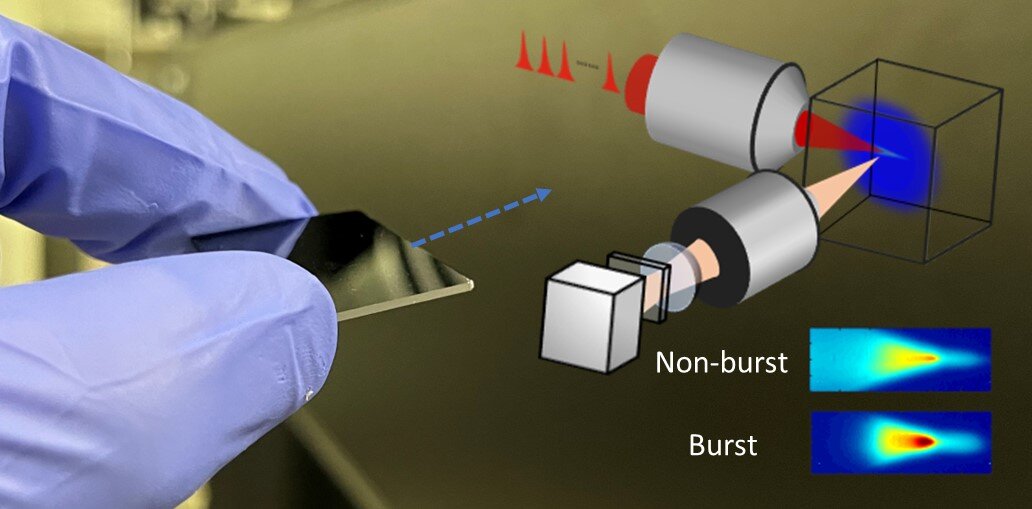
Researchers from French National Center for Scientific Research (CNRS, LP3 Lab) split the energy of infrared ultrafast pulses to form ultrafast bursts of less intense pulses, to achieve better localization of excitation. Bursts of a sufficient speed enable the accumulation of enough energy to cross the material modification threshold and, thus, locally add new functionalities inside semiconductor chips. Courtesy of Andong Wang, Pol Sopeña, and David Grojo.
The team used an infrared wavelength similar to that used for telecommunications to penetrate the semiconductor material. With the proper wavelength selected, the team had to address other physical limitations — with the use of intense light such as that required for material processing, highly efficient nonlinear ionization inside narrow gap materials creates free electrons inside the material. This will rapidly transform any semiconductor into metal-like materials, which makes it impossible to propagate light deep inside the matter. This transition deteriorates the focusing process and prevents the occurrence of material modification using ultrafast lasers.
To address this, the team proposed the use of nonconventional ultrafast bursts of pulses to circumvent the metallization transition.
According to Andong Wang, an investigator on the research, previous demonstrations used light pulses that were too strong and that excited the electrons too easily. In the recent work, Wang and the team split the pulse energy into a large number of weaker pulses with an extremely fast repetition rate. “These pulse trains, also called bursts, will avoid strong pulse excitation before the light is focused,” Wang said. “Additionally, the pulses will repeat very fast so that the delivered laser energy can accumulate efficiently to cross the modification.”
According to team leader David Grojo, the demonstration offered the first very practical solution for ultrafast laser writing inside semiconductors. The next step, Grojo said, will be to concentrate on the type of modifications that can be achieved inside these materials.
“Refractive index engineering is surely an important target given the growing importance of silicon photonics,” Grojo said. “Laser writing would offer the possibility of direct digital fabrication of 3D architecture materials inaccessible by current manufacturing technologies. In the future, these new laser modalities may drastically change the way advanced microchips are today fabricated.”
The research was published in International Journal of Extreme Manufacturing (www.dx.doi.org/10.1088/2631-7990/ac8fc3).