NTT and the Tokyo Institute of Technology (Tokyo Tech) have developed an all-optical switch that operates in the ultrafast regime with a response time in the femtosecond (fs) range and with energy consumption in the femtojoule (fJ) range. To achieve both speed and energy efficiency in the switching, the researchers combined a nanosize optical waveguide based on plasmonics with graphene.
All-optical switches are expected to operate faster than switches that are electrically controlled. However, the switching energies of all-optical switches are relatively high. For ultrafast information processing, optical components need to be densely integrated in photonic circuits, and the energy consumption of each device must be low.
The researchers used graphene because it has an ultrafast nonlinear optical response and a large absorption coefficient over a broadband wavelength range.
Monolayer graphene absorbs 2.3% of light over a wavelength range from the visible to infrared, giving it a much larger absorption coefficient than conventional semiconductors. In addition, graphene shows saturable absorption and a nonlinear optical effect, and its response time can be less than 100 fs. This ultrafast response originates from the very short relaxation times of graphene carriers, the researchers said.
In the new all-optical switch, a transmittance change induced by saturable absorption switches the on/off state, and the absorption saturates as a result of photo-excited carriers.
However, graphene is only 1 atom thick — too thin for optical devices, according to the team. Further, the interaction between graphene and light is weak when a conventional waveguide made of silicon is used, which could increase energy consumption. The research team overcame this problem by strongly confining light within a nanoscale plasmonic waveguide. With a core width of only 30 nm and a height of only 20 nm, the core area of the waveguide was as small as λ2/4000 (wavelength λ; in this case the wavelength was 1550 nm).
The absorption coefficient for a plasmonic waveguide with a core size of 30 × 20 nm is estimated to be much higher than for a graphene-loaded silicon waveguide with a core measuring 400 × 200 nm. This enabled the researchers to decrease the device length. Further, light intensity at the position of the graphene in a plasmonic waveguide is 310× larger than it would be in a silicon waveguide, because the plasmonic waveguide core is much smaller. This enhancement significantly reduced the energy required for switching, the team said.
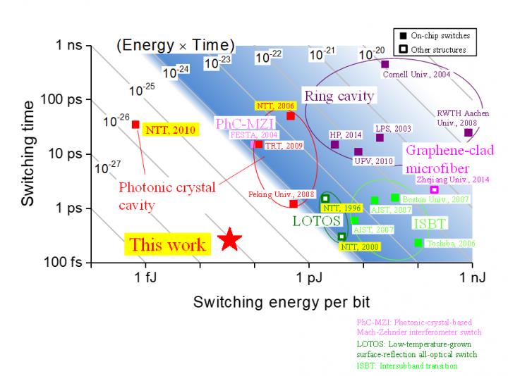
A comparison and performance of different optical switching architectures. Courtesy of NTT, Tokyo Tech.
The researchers loaded graphene on the plasmonic waveguides using nanofabrication technologies developed by NTT. The cross-sectional area of these plasmonic waveguides was about 1/100th that of what would be considered compact silicon waveguides, and about 1/105th that of single-mode optical fibers.
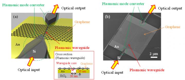
The researchers propose an all-optical switch that consists of graphene-loaded MIM-WGs equipped with plasmonic mode converters connected to Si-WGs. Courtesy of NTT, Tokyo Tech.
The experimentally obtained absorption coefficient for the graphene-loaded plasmonic waveguide was 1.7 dB/μm. The obtained saturation energy was 12 fJ, which is four orders of magnitude smaller than a graphene-loaded silicon waveguide. Because an increase in light intensity can be regarded as a reduction of the saturation energy in saturable absorption, this result means that the light intensity was enhanced by four orders of magnitude. The new all-optical switch demonstrated a switching time of 260 fs, which was achieved with a switching energy of 35 fJ. According to the researchers, the switching energy is the smallest value ever reported (1/100th of that previously reported) for any type of all-optical switch operating at less than one picosecond.
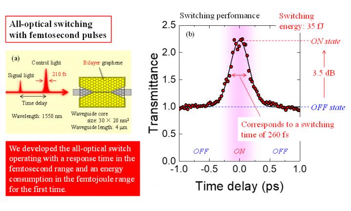
The signal light is switched on/off with a control light. In the TokyoTech/NTT switch, the control light induces a nonlinear optical effect of graphene; that is, it changes the degree of absorption by graphene. A switching time of 260 fs can be achieved with a switching energy of 35 fJ. Courtesy of NTT, Tokyo Tech.
The researchers hope that their all-optical switch will be used in future photonic integrated circuits for ultrafast information processing. The nanoscale waveguide of the switch could also serve as a platform for developing nanophotonic information processing devices incorporating nanowires and other 2D materials. Further, the all-optical switching device could be used as a nonlinear activation function in optical neural networks. In the future, the researchers plan to increase the performance of the all-optical switch, apply the technology to other photonic devices such as detectors, and explore the use of other nanomaterials for building the device.
The research was published in Nature Photonics (www.doi.org/10.1038/s41566-019-0547-7).