A deep look into the micro- and nanoscales reveals how 3D microprinting is changing the design and manufacturing processes of precision components.
SOFÍA RODRÍGUEZ, NANOSCRIBE GmbH
Miniaturization is the trend of downsizing devices and products, which is triggering technological innovation. Miniaturization down to the microscale means functional components are becoming even smaller and lighter and increasing the performance of highly integrated systems. For example, miniaturized photonic chips, cameras, and sensor systems enable
applications ranging from high-speed data- and telecommunications to ultracompact imaging systems in mobile devices and disposable medical instrumentation at the point of care. These applications require new manufacturing and packaging methods to bring more and more miniaturized and high-performance components together in increasingly small spaces. Here, additive manufacturing (AM) with submicrometer precision provides an interesting value proposition.
Various 3D-printing technologies are
already available for fabricating 3D
objects at the macroscopic scale, including fused deposition modeling, selective laser sintering, and stereolithography. These technologies speed up innovation cycles in scientific as well as industrial applications and have — in some cases — even replaced traditional subtractive manufacturing.
However, when fabricating miniaturized components, conventional AM technologies are not consistently delivering the resolution and precision required in photonics and micro-optics. Two-photon polymerization (2PP) was experimentally introduced in 1997 by Satoshi Kawata
and colleagues. It has now reached maturity; 2PP-based 3D-printing technology offers the design freedom and traditional workflow known from 3D-printing standards, while performing with 100-fold higher resolution and smaller feature sizes than conventional printers.
During these last two decades, 2PP-based 3D microprinting has entered application fields ranging from photonic crystals and metamaterials to refractive micro-optics (Figure 1) and diffractive optical elements. After improvements
in the fabrication strategy, as well as
the development of novel software and hardware features, the 2PP-based technique allows the production of 3D micro-structures in situ, exactly where they are needed, on a broad range of objects and devices, including micro-optics on photonic chips and even on the tips of optical fibers.
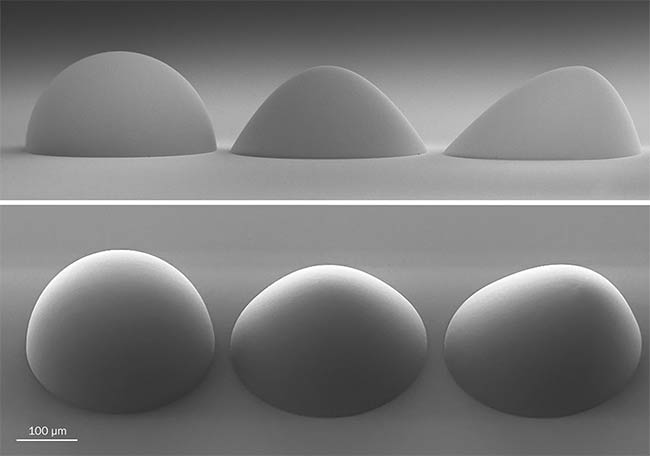
Figure 1. (From left) 3D-printed hemispherical lens, aspheric lens, and freeform asymmetric lens.
On-chip 3D printing
Conventional packaging methods require several steps to assemble various components on one microchip, whereas 2PP-based 3D microprinters can fabricate highly precise microparts directly onto a photonic integrated circuit without any further assembly, alignment, pick and place, or fixing steps. In situ fabrication by means of 3D microprinting reduces packaging costs and saves time by incorporating components with precision.
In situ fabrication is made possible by a dip-in configuration of the 3D-printing process. The technique exploits the fact that a liquid resin can be applied by drop on a substrate, and then the writing laser beam only affects the photoresin in the focus, not above or below the focal volume. In this configuration, the photosensitive material works as an immersion liquid for the focusing optics, which in turn enables simultaneous imaging and printing at well-defined positions, with respect to patterns and markers on the photonic circuit.
A typical process starts with the preparation of the print job from a 3D CAD model using a recipe that may include optimized slicing and hatching parameters. Then the laser beam solidifies the resin within a tight focal volume and scans the resin by means of an ultrafast galvo scanner along the trajectories of the 3D design (Figure 2), forming a 3D part.
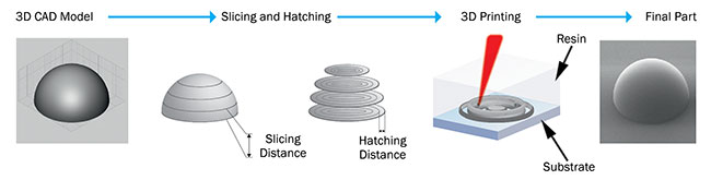
Figure 2. 3D printing workflow from 3D CAD model to final part. The printer software imports a CAD design and compiles a print job with slicing and hatching parameters for the 3D-printing process. The final result is a 3D-printed part immersed in a developer bath to remove the unpolymerized material.
Printing microlenses onto photonic chips is one example. A series of hemispherical microlenses was fabricated on top of grating couplers that were previously patterned onto the chip (Figure 3). There the microlenses can couple light into the photonic circuit. In one continuous printing step, the 3D printer fabricates the microlenses without the need to align or mount the finished elements mechanically. The final printed microlenses are fabricated additively with submicron precision, which results in optical-quality surfaces.
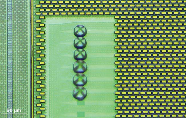
Figure 3. Optical microscope image of the 3D-printed hemispherical lenses on a photonic chip.
3D-printed micro-optical components also find applications in the field of optofluidics. Highly precise fabrication and positioning of optical components are needed for coupling light between miniaturized light sources and detectors to optically measure the properties of a fluid passing between them.
In a recent paper1, researchers showed the fabrication of astigmatic aspheric beam-shaping microlenses. They printed microlenses directly onto vertical laser
facets that were separated by a 200-µm-wide microfluidic channel. The incorporation of the aspheric microlenses onto the chip via in situ 3D printing increased the coupling efficiency by 12.6 dB compared to integrated circuits without the lenses. The resulting microfluidic system could be used for examining human blood cells in lab-on-a-chip applications.
On-fiber multilens assembly
3D printing on prepatterned devices is a practical substitute for the process of mounting and assembling optical elements on the narrow tips of glass fibers. Relevant application cases are doublet or triplet lens systems that can be directly 3D-printed on imaging fibers and small imaging chips. 3D-printed microlenses pave the way for the miniaturization of endoscopy systems, which can potentially find medical applications through millimeter-sized body orifices.
An objective lens system2 can be 3D-printed directly on the end facet of a fiber (Figure 4). Using the direct layer-by-layer 3D-printing approach, the compound lens system was produced in one single printing step without the need for further assembly or alignment of the lenses — process steps that are known for very low yield.
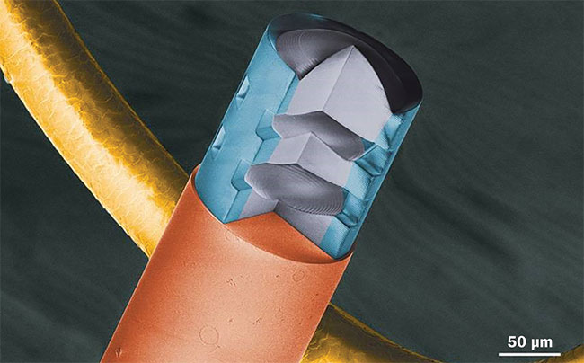
Figure 4. Colored scanning electron microscopy (SEM) image of a multilens assembly on the tip of a fiber.
Taking these results further, a consortium consisting of the endoscope manufacturer KARL STORZ, the 3D microprinter supplier Nanoscribe, and the University of Stuttgart investigates complex 3D-microprinted optical systems within a publicly funded project, PRINTOPTICS. The goal of this project, started in 2016, is to employ 3D printing to
produce complex yet miniaturized optics that remain difficult to fabricate by
means of injection molding or other established manufacturing methods. The project aims to demonstrate that the 2PP-based 3D-printing process is suitable for producing high-quality endoscopy systems.
3D-printed refractive micro-optics
3D microprinting can also open new ways to fabricate single lenses or microlens arrays with shapes that were, until a few years ago, hard or impossible to manufacture. For these applications, the 3D-printed micro-optics can operate as final parts as well as polymer masters for subsequent mass replication — for example, by injection molding or nanoimprint lithography. Here, the combination of a 3D microprinter, a printable resin material designed for smooth surfaces, and high shape accuracy is able to deliver micro-optical elements with a surface roughness >10 nm Ra and a shape accuracy >1 µm (peak-to-valley value).
Since 2PP is a tool-free AM method, it overcomes the design constraints of subtractive techniques such as diamond milling, which uses a mechanical object to remove material from a workpiece. As shown in the example of hemispherical microlenses (Figure 3), the surfaces of
the printed microlenses can have a slope ranging from 0° to 90°, even with extremely small distances of a few micrometers between the lenses and a very high uniformity among the elements within the microlens array. Even microlens arrays with overlapping lenses, 100 percent filling factor, and arbitrary surface profiles can be printed.
3D microprinting is also versatile enough to be used to realize concave microlens arrays. It can be used to fabricate concave microlens arrays with deep sags of 40-µm depth and sharp tips for diffuser applications3. The printed microlenses are used as masters for replication into polymethyl methacrylate (PMMA) by an intermediate negative mold in polydimethylsiloxane (PDMS).
Further optical components can be printed with features such as sharp edges and angles or even full 3D designs. Micro-lenses, prisms, corner cube arrays, and other freeform optical elements can thus be fabricated in an additive way.
Additively manufactured DOEs
3D microprinting of refractive optics relies on the high precision and shape accuracy offered by the 2PP technique. Likewise, 3D microprinters offer the possibility to fabricate submicron feature sizes required when diffractive optical
elements (DOEs) are to be produced. DOEs are devices whose micro- or nanostructured surfaces modulate light by diffraction. They can generate almost arbitrary light distributions in the far field that have applications in beam shaping, beam homogenizing, and beamsplitting.
Optical security devices may incorporate, for example, transparent DOEs. These generate an image when illuminated with coherent light from a laser source and can be used as easy-to-check, human-readable anticounterfeiting labels.
Typically, binary or multilevel DOEs, or the master for replicating them, are made by means of lithographic techniques and etching processes. A drawback of these fabrication processes is the need
for multiple lithography and etch steps and critical alignment procedures before each lithography step. Compared to these
processes, 3D microprinting offers a quick, cost-effective workflow for producing optically complex prototypes and polymer masters of DOEs in one printing step.
A phase distribution image of a DOE, previously computed by an external program, is required for the print preparation. Once this is done, the printer software imports the phase distribution image in the form of a bitmap. It then generates a height profile with the use of a recipe that includes optimized print parameters, such as layer distance and print speed. After the preparation, the 3D microprinter produces the designed DOE as a 2.5D relief structure, layer by layer, in a single print run.
3D biomedical devices
Another field driven by miniaturization is medicine, where minimally invasive procedures gain relevance in diagnostics, therapeutic applications, and health monitoring. Remotely controlled microrobots are envisioned for complex biomedical applications where space is minute, such as in the handling of drug delivery and single cells or biological tissue.
A concept for remote control and actuation that is actively pursued in academia uses miniaturized magnetic helices. When submerged in a liquid and subjected to the appropriate magnetic fields, these start to rotate around the helix axis and generate propulsion. Control over the magnetic field’s orientation allows steering of the helices.
Several designs exist that use small cages at the tip of the helix or use the helix itself for transporting biologically or clinically relevant cargo. The procedure for making these helices relies on using 2PP to 3D-print the helix. Usually, polymeric helices are printed and then coated with ferromagnetic nickel and a thin titanium coating for biocompatibility. However, materials based on a mixture of hydrogels and magnetic nanoparticles have also been used successfully. These have the advantage of being biodegradable and loadable with pharmaceutically active compounds by simple immersion in a solution.
Another example of a biomedical device made using 2PP is a multicomponent nerve interface implant developed and 3D-printed at Boston University4 to stimulate and track nerve responses. The microscale implant, also called a nanoclip (Figure 5), has many features, including trapdoors for fixing a nerve, slots for placing electrodes, and through-holes for surgical handling. After being 3D-printed, it was transplanted into a zebra finch to show nerve activity post implant without harming the living bird.
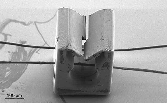
Figure 5. Nerve interface implant for tracking nerve responses.
Outlook
The use of 3D microprinting helps overcome limitations when fabricating miniaturized complex designs at the nano- and microscale. In many sectors, this AM technology develops rapidly, changing the manufacturing strategies of integrated photonics, micro-optics, and biomedical devices.
Two-photon polymerization systems enable the direct fabrication of 3D structures on premanufactured devices such as photonic integrated circuits and optical fibers. The same device offers the high precision needed for smooth refractive optics and the submicron feature sizes required in multilevel diffractive optical elements. The 3D microprinting approach can be exploited for the assembly-free fabrication of complex 3D parts, opening the way to new applications, such as compound lens systems, drug-delivery micromachines, and implantable devices. Because of their characteristic design freedom and simple workflow, 3D microprinters continue to expand the possibilities of producing a variety of nano- and microstructures.
Meet the author
Sofía Rodríguez develops product- and applications-related content at Nanoscribe GmbH. She studied physics at the Julius-Maximilians-Universität Würzburg (Germany); email:
[email protected].
References
1. R. Thomas et al. (2018). In situ fabricated 3D micro-lenses for photonic integrated circuits. Opt Express, Vol. 26, Issue 10,
pp. 13436-13442.
2. T. Gissibl et al. (2016). Sub-micrometre accurate free-form optics by three-dimensional printing on single-mode fibres. Nat Commun 7, Article no. 11763, https://doi.org/10.1038/ncomms11763.
3. R. Kirchner et al. (2018). Benchmarking surface selective vacuum ultraviolet and thermal postprocessing of thermoplastics for ultrasmooth 3-D-printed micro-optics. Opt Eng, Vol. 57, Issue 4, 041403, https://doi.org/10.1117/1.OE.57.4.041403.
4. C.A. Lissandrello et al. (2017). A micro-scale printable nanoclip for electrical stimulation and recording in small nerves. J Neural Eng, Vol. 14, Issue 3, https://doi.org/10.1088/1741-2552/aa5a5b.