Better performance, lower cost
Art Stout, Sofradir EC Inc.
Infrared camera manufacturers can choose from a wide variety of uncooled IR detectors to make different model designs for a variety of commercial, industrial and military products.
Uncooled infrared detectors have seen many significant technology advances – improved reliability, better manufacturability and lower costs – that have fueled the availability of a wide variety of IR cameras. Low-cost portable and fixed infrared cameras as well as high-performance systems have been introduced for a variety of thermal imaging applications.
Thanks to new price points and better overall performance, traditional markets for infrared cameras have exploded, while new markets have been created.
Uncooled detectors go mainstream
There are two classes of infrared detectors that can be used to manufacture IR cameras: cooled and uncooled. Cooled detectors – named for their reliance on a cryogenic cooling mechanism – are considered extraordinarily sensitive to infrared radiation. The cryocooler substantially reduces thermal noise (infrared radiation from sources other than the objects being observed) down to very low levels. Mercury cadmium telluride and indium antimonide are the most common materials used in cooled detectors. Because the cryocooler unit is a mechanical device with moving parts, cooled detectors usually require maintenance after a period of time, often for every 8000 to 10,000 hours of operation.
Uncooled infrared detectors have become an excellent alternative and are much more commonly used in many commercial, industrial and military IR camera products. Because they do not require the use of a cryogenic cooling unit, infrared cameras that use uncooled detectors enjoy substantial advantages in maintainability as well as a significant reduction in size, complexity and cost.
The primary type of uncooled detector today is the microbolometer, a device based on microelectromechanical systems technology. When infrared radiation in the wavelength range between 7 and 13 µm strikes the microbolometer’s detector material and is absorbed, it heats up, and the resulting change in its electrical resistance is the basic sensing technique. These changes are processed by separate core electronics to create a thermal image. These detectors are quite sensitive and can sense heat radiated from objects, depending upon their temperature.

This thermal image obtained with a 1024 × 768 a-Si microbolometer detector shows both high sensitivity and high resolution. Courtesy of ULIS (sister company to Sofradir).
The two most common microbolometer detector materials are amorphous silicon (a-Si) and vanadium oxide, referring to the material on the outermost thin-film layer. While the two materials function in a similar manner, there are many differences between them.
Microbolometers having a-Si as the thermometer material have been developed using sophisticated surface micromachining techniques to produce very thin, very sensitive membranes. These detectors can be economically used in an extremely thin ceramic package specifically designed for the detector. The array is integrated and subsequently sealed under vacuum without the need for any pinch-off tube. The design of the detector package allows for a 15-year storage lifetime at room temperature.
These detectors have become widely integrated into many commercial and military products. Because of the use of a-Si, they have benefited from widely available silicon manufacturing processes. They also have benefited from a great deal of research on improving the performance of similar silicon-based devices, such as solar cells and flat panel displays, with particular attention to pixel operability and uniformity. Although other detector materials such as vanadium oxide have shown slightly better noise figures, the technological benefits of a-Si pixels and high-yield silicon manufacturing processes have rapidly popularized this technology.
Technological advancements
Technological breakthroughs in a-Si microbolometers have occurred at a constant pace, resulting in performance improvements such as resolution and sensitivity as well as in better detector packaging. Pixel uniformity and operability due to production changes have continued to improve as well.
1. Reduced pixel geometries
Because a-Si is inherently stiff, microbolometers manufactured with this material can be made with very small bridge structures. As a result of these thinner membranes, a-Si microbolometers exhibit higher effective thermal insulation than devices based on vanadium oxide. Reduced bridge size allows also for the development of small pixels and therefore more pixels per area, smaller physical sizes and lower costs. The a-Si microbolometer pixel is quite simple in structure, so reducing pixel size does not require a complex microbridge, since the structure scales appropriately. As a result, the number of fabrication operations in the manufacturing process is optimized.
Over the past 10 years, a-Si infrared detector arrays have seen a steady reduction in pixel pitch from 45 µm back in 2000 to 17 µm in 2008. Next-generation arrays are projected to have a 12-µm-pixel pitch geometry, further reducing the size of detectors and optics as well as the size of infrared cameras.
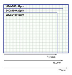
As pixel pitch decreases and pixel counts increase, the detector active area stays fairly stable.
In conjunction with pixel pitch reductions, arrays offering higher resolution have been introduced. Many microbolometer array sizes are available, from a low-resolution 160 × 120 array to a large-format 1024 × 768 array. In light of the reduction in pixel size and the increase in resolution, the active detection area for these arrays remains nearly constant for certain comparative array sizes. The width of a detector having 320 × 240 pixels with 45-μm pixels (14.4 mm) is quite similar to the width of a detector having 640 × 480 pixels with 25-μm pixels (16.0 mm) and also to the width of a detector having 1024 × 768 pixels with 17-μm pixels (17.4 mm). With similar detection areas, production and packaging costs are maintained, and the size and cost of infrared camera housings and optics can be stabilized.
2. Thermal time constant and sensitivity
Thermal time constant is one of the most important parameters in the design of an infrared imaging detector, exceeding the importance of other parameters. Again, because of the intrinsic properties of silicon, a-Si pixels can be produced with very thin microstructures because of their rigid behavior. With these thin microstructures, pixels exhibit a very low thermal conductance between the pixel and substrate, and low suspended thermal pixel mass. This results in pixels having a very short time constant and very fast response time, which is an enormous benefit for any infrared detector. It is commonly accepted that pixel response times should not exceed one-third of the reciprocal of the frame time (i.e., 10 ms for an array operating at 30 Hz). This is easily achieved with a-Si pixels.
As pixel pitch decreases, other parameters must be appropriately modified to keep pixel sensitivity from decreasing as the active detection area becomes smaller. Because sensitivity has a great impact on image quality, certain design changes are important to ensure that detector sensitivity remains at the desired level. For example, when the pixel pitch of a-Si microbolometers was reduced from 45 to 25 µm, the photolithographic resolution improved with no adverse impact on fill factor. While 1.5-μm minimum design rules were used for 45-μm pitch detectors, 25-μm detectors required 0.8-μm minimum design rules, and 0.5 μm for 17-μm pitch detectors. However, improvements in the design of the support legs as well as a reduction in both the width and thickness of the patterned legs resulted in higher thermal insulation. The result was a microbolometer array having the same sensitivity but with all the advantages of smaller pixels.
To further reduce the pixel pitch while maintaining pixel time constant and detector sensitivity, pixel design modifications were required. It was necessary to reduce the thickness of the microbridge films to reduce their thermal mass. To maintain good noise immunity, the microbridge was thinned down at the same rate of decrease as the detector active area. At the same time (but more challenging), the thermal conductance also had to be reduced at a rate corresponding to the square of the pixel area. Because of the simplicity of the silicon substrate, the thickness of the a-Si microbridge could be easily reduced with very few restrictions.
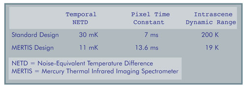
As an example of the importance of pixel time constant, compare the results of different a-Si focal planes as shown in the table: One is standard in design, and another is designed for high-sensitivity, narrow intra-scene dynamic range applications such as would be required in astronomical missions.
 3. Image uniformity and operability
As with other imaging arrays, each microbolometer pixel has a slightly different response given by the pixel gain and pixel offset. During the manufacturing process, each array has a resulting distribution of gain and offset values from each pixel. Because of well-established silicon manufacturing methods and the simplicity of the a-Si microbolometer’s structure, the device exhibits excellent image uniformity, as shown by the similar behavior of all the pixels. Excellent array uniformity means that the array gain can be increased before digitization to improve overall system signal-to-noise performance.
The operability of an IR detector array is defined by the number, or percentage, of defective pixels in the array. Highly uniform arrays have a smaller number of bad pixels since pixels are defined as defective if their characteristics are significantly different from the average. To achieve the best image, array pixel response should be as uniform as possible across the surface of the device prior to any nonuniformity correction. Amorphous silicon detectors traditionally offer high operability rates because of the simplicity of silicon technology and the benefits of established processes. Operability of better than 99.5 percent is standard in a-Si detectors, and rates as high as 99.9 percent are not uncommon.
Amorphous silicon detectors are well-known for their excellent array uniformity, resulting in improved image quality, reduced system complexity and lower overall costs.
Because of their intrinsic uniformity, a-Si detectors have other important advantages over other types of microbolometer detectors. For example, they can be operated quite easily without a thermoelectric cooler. Since a-Si pixels have only one activation energy that defines the bolometer resistance as a function of temperature, knowing the pixel resistance at one temperature is sufficient for predicting the resistance at other temperatures.
Microbolometer arrays manufactured with a composite of materials (e.g., vanadium oxide) have numerous factors that affect the response of the pixels in the array and are not so easily characterized. Consequently, they exhibit higher nonuniformity characteristics and are more difficult to operate in a mode without a thermoelectric cooler since the wide variation in response cannot be easily predicted. In addition, if not appropriately compensated, some of the pixels in the array may appear saturated, having a response outside the detector digitization range. Because of the high uniformity of a-Si detector arrays, the raw signal delivered by the detector is sufficiently uniform to be processed without any additional electronics, which reduces system complexity, calibration, yield, power consumption, size and cost.
Applications
High performance, high reliability and lower cost make a-Si detectors ideally suited for many IR applications in both commercial and military sectors. IR detectors and cameras are now becoming standard in automobiles as night-vision systems. Thermal imaging cameras also have been used to find victims in live fires and for airport “fever screening.”
Because of technological advances such as 17-μm pixel pitch and large-format detectors, a-Si microbolometers are finding their way into many more military and commercial night-vision applications, including security and basic surveillance. For example, unmanned aerial vehicles require lightweight and reliable IR detectors that can stand physical punishment including high vibrations and high g force loads. These requirements make uncooled a-Si microbolometers ideally suited for this application.
Certain IR cameras can be calibrated to provide noncontact measurement of object temperature. These can be used for industrial inspection, especially in environments with high power usage. Inspectors use IR cameras for thermal analysis to detect and prevent problems with electrical and mechanical components. In these systems, excess heat can be a sign of a potential problem, so noninvasive infrared cameras scan for issues including loose or dirty connections, overloaded circuits and plugged cooling lines in transformers.
IR detectors and thermal imaging provide an easy-to-use tool for conducting energy audits. These focus primarily on insulation and seals around exterior doors and windows as well as on gaps or cracks that are leaking energy. In addition, thermal imaging cameras can save time and money in detecting pipe leaks: A quick scan can eliminate the need for destroying a wall or digging up a pipe.
Meet the author
Art Stout is vice president of business development at Sofradir EC Inc. in Fairfield, N.J.; e-mail: [email protected].
References
1. J.J. Yon et al (May 2008). Latest amorphous silicon microbolometer developments at LETI-LIR. Proc SPIE, pp. 69401W-69401W-8.
2. C. Trouilleau et al (May 6, 2009). High-performance uncooled amorphous silicon TEC less XGA IRFPA with 17-µm pixel pitch. Proc SPIE, Vol. 7298.