Growing demand from automotive and consumer applications is driving improvements to VCSEL power density and cost, encouraging developments at eye-safe wavelengths.
For vertical-cavity surface-emitting lasers (VCSELs),
the future looks bright — because their performance is rising while their price is falling. On the horizon is also a move from near-IR to shortwave IR
wavelengths. These trends will help VCSELs meet a surging demand that is driven by their increasing use in 3D
sensing applications (Figure 1).
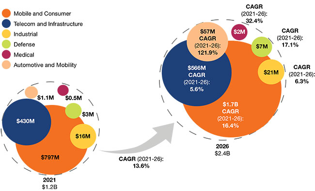
Figure 1. The VCSEL market forecast for 2021 to 2026, according to a 2021 Yole Développement report on market trends for the technology. Mobile and consumer applications remain the largest market for VCSELs, while automotive and mobility uses are growing rapidly. CAGR: compound annual growth rate. Courtesy of Yole Développement.
“It started in smartphones more than five years ago,” said Pierrick Boulay, senior technology and market analyst in the Photonics and Sensing Division at Yole Développement. “But it is starting to enter in automotive and also in industrial applications — mostly related to the autonomy of the logistics chain — such as forklifts, automated guided vehicles, trucks, delivery robots, and so on, and in smart infrastructure applications for traffic monitoring and people monitoring.”
In automotive, a primary application is forward-looking lidar, as well as rear- and side-looking. 3D sensing is also used inside the vehicle cabin. Lidar that peers ahead of a car needs a high-power light source because the system must detect objects at great distances, while rear and side lidar use a lower-power light source for shorter 3D sensing ranges, as do those for in-cabin applications.
3D sensing is achieved using various approaches, such as time of flight and structured light. Time-of-flight techniques are used in lidar and some automotive applications — to determine distance by measuring how long light takes to travel to and from an object, for example (Figure 2). Structured light, which is used in mobile phone facial recognition and elsewhere, projects a pattern onto an object and then calculates relative depth information from distortions in the reflected pattern.
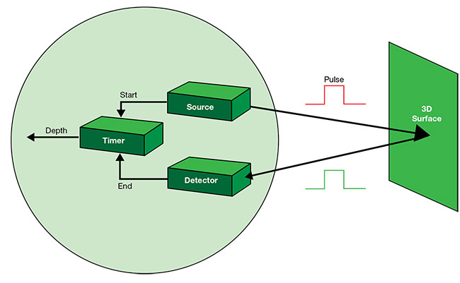
Figure 2. Time-of-flight sensing is widely used in automotive applications — for example, to determine the distance to another vehicle or an object. Courtesy of Lumentum.
Improving VCSEL efficiency
The VCSEL’s journey to supporting large-scale demand for high-performing 3D sensing is a tale of many advancements. André Wong, vice president of product line management for 3D sensing at Lumentum, said the term “VCSEL” sometimes refers to a single emitter, but for 3D sensing, customers want to buy an array of VCSELs on a single chip.
A VCSEL array on a chip that has a footprint of up to 1 × 1 mm typically comprises hundreds of emitters with output powers ranging from milliwatts to several watts for 3D sensing in mobile devices, said Gerald Dahlmann, director of strategic marketing for consumer electronics at II-VI.
Companies have demonstrated larger chips with arrays comprising up to thousands of emitters and power in the tens
of watts, suitable for long-range lidar. Wavelengths for all these devices are
in the near-IR range, usually at 850 or 940 nm.
About a decade ago, manufacturers expanded the gallium arsenide (GaAs) wafers used to make VCSELs from 100 to 150 mm in diameter, more than doubling the number of chips per wafer and reducing manufacturing costs per chip, Wong said. In the years since, vendors have improved device power density by implementing multilayer junctions to multiply photon production. Another advancement, multilayer metal, has improved individual emitter addressing capabilities, which has enabled dynamic optimization of illumination for 3D sensing.
Vendors have also added options to tailor the beam shape and change its characteristics, such as its polarization (Figure 3). Controllable, polarized light improves the illumination quality and resolution in demanding 3D applications, said Ralph Gudde, vice president of marketing and sales at TRUMPF Photonic Components.
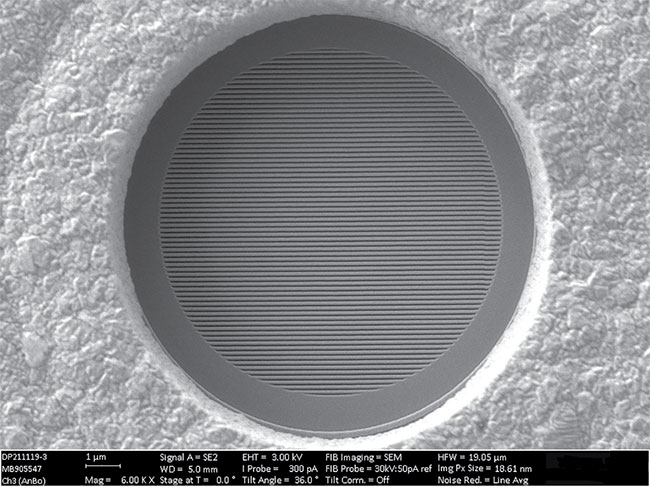
Figure 3. A scanning electron microscopy image of a polarization-locked grating. Controlling polarization helps meet demanding VCSEL illumination specifications. Courtesy of TRUMPF.
“High-end smartphone applications demand a constant development in functionalities of lasers for time-of-flight or structured light, to improve applications such as face recognition or laser autofocus,” Gudde said.
Managing heat and power density
Each improvement has included limitations and new requirements, however. Increasing the wafer size has required retooling factories and establishing sources for the larger wafers, which therefore has increased coordination among wafer vendors, VCSEL manufacturing system makers, and VCSEL producers.
Multilayer junctions multiply not only photon production but also heat production. Wong said Lumentum stacks as many as six junction emitters to deliver a power density that is adequate for automotive applications (Figure 4). However, when designing a solution, engineers must balance an application’s need for power with the competing need to eliminate waste heat.
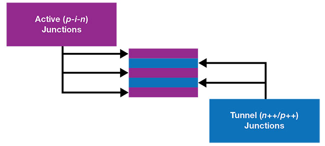
Figure 4. Multijunction VCSELs stack emission regions to increase photon production per chip.
Courtesy of Lumentum.
Software solves this problem in some applications, he said. Pulsing the output reduces the average power (and waste heat) while preserving peak power. For individually addressable VCSEL arrays, software can shut off all or part of the array, adjusting the pulsed operation to achieve application requirements.
The issue of dissipating heat also arises when feature sizes must shrink to manage system packaging size. The state-of-the-art feature size for VCSELs currently stands at a few tens of microns for a single emitter. By shrinking emitters and other system components, manufacturers
pack more individual VCSELs into a chip without increasing the chip size. The increased output power density benefits 3D sensing.
“Improving your power per unit area is all about shrinking your system size and making your systems more efficient,” Wong said. “In these sensing applications, the most important thing is your signal-to-noise ratio: How much power are you getting on your subject? How much can you get back?”
Benefits at longer wavelengths
According to Wong, another key factor that affects signal-to-noise ratio is the sensor performance. If a sensor detects light more efficiently, the source can
emit less light. Hence, advancements in sensors spur innovations and improvements in VCSELs.
Wong said Sony has developed a sensor device that covers the spectrum from
400 to 1700 nm by layering indium phosphide (InP), for shortwave IR light, atop indium gallium arsenide (InGaAs), for visible light.
Yole Développement’s Boulay said the upper end of this range is important because the OLEDs used in displays are transparent at 1300- to 1400-nm wavelengths. This makes it possible to hide a 3D sensor within a smartphone — for example, beneath the display. Today, 3D sensing uses 940-nm VCSELs with sensors that are sensitive to that wavelength and require a small cutout in the display.
Longer wavelengths also enhance eye safety. Although people cannot see light in the near-IR, exposure to it, when it is intense enough, damages the eye. As 3D sensing applications increase and power levels grow, such exposure is more likely. Shifting 3D sensing to a longer wavelength minimizes or effectively eliminates this hazard.
Also, background light is limited near 1400 nm. This results in both lower noise and the potential to increase power, which is currently limited by the need for eye safety. “Signal-to-noise ratio can be improved, which enables higher resolution and longer range,” II-VI’s Dahlmann said.
VCSELs for the SWIR
If VCSELs are to survive a shift into the SWIR, device manufacturers need
a material that generates photons near 1400 nm, which current GaAs VCSELs cannot achieve. Researchers and companies are therefore investigating nitride-based GaAs VCSEL formulations, as well as other new materials. Long-wavelength VCSEL-maker VERTILAS recently
announced an InP-based array that emits 8 W of quasi-continuous power at
1300 nm. This power level is close to
that which is currently used for near-IR short-range 3D sensing applications, such as facial recognition in mobile phones.
Semiconductor wafer manufacturer IQE announced that it achieved the power and longevity milestones needed in nitride-based GaAs technologies for 3D sensing in the SWIR. The company is working with partners to refine the technology and ready it for production.
These new materials face challenges. InP wafers are one-third to one-half the diameter of GaAs wafers, giving one-quarter the possible die per wafer, compared to GaAs wafers using a die of the same size. This difference translates into a higher manufacturing cost for an InP-based device, all things being equal.
Another potential issue for these new materials involves gaining market acceptance. For example, automotive applications require substantial proof that VCSELs meet demanding performance and reliability specifications. Some time
may therefore be required for longer-wavelength VCSELs to gain traction in these applications.
“Changes are incremental. There is no revolution in technologies,” Boulay said, adding that the market may split, with consumer applications embracing longer-wavelength VCSELs while the industrial and automotive sectors continue to use near-IR solutions.
Even with these hurdles, SWIR VCSELs are on the horizon. Major producers are watching and developing longer-wavelength offerings. Lumentum and II-VI are actively developing SWIR technology, Boulay said. Teaming up with sensor-maker Artilux, Lumentum in March demonstrated a 940- and 1380-nm NIR/SWIR platform that has initial
applications in biosensing and biometrics. Gudde said TRUMPF is also exploring opportunities to serve early-stage SWIR market development.
3D sensing for virtual spaces
To sum up his thoughts regarding the future for VCSELs, Wong brought up the concept of the metaverse, a virtual reality space where users interact with a computer-generated environment and other users. The technology to achieve this space requires expanded 3D sensing capabilities. “VCSELs will be a key part of that,” he said.