The technology allows for mass production in industries that demand high performance and specialized design.
Martin Eibelhuber, Robert Breyer, and Mikhail Begel, EV Group
For many years, innovations in sensors for mass markets such as automotive, gaming, and consumer electronics have been driven by the microelectromechanical systems (MEMS) industry. MEMS-based sensors are well known to provide solutions for a multitude of applications that require the smallest form factors or size of components and packaging, while still providing high performance. However, emerging markets for autonomous vehicles, augmented reality, biomedical uses, and security solutions have necessitated a focus on optical sensors and projectors to their product requirements. By measuring intensity, wavelength, or polarization and the respective change of the light, it is possible to identify nearly any physical property of an object or the environment, and it is even possible to gain chemical information.
Still, it is a challenge to miniaturize optical sensing components to dimensions that allow sensors to fit in any device and be manufactured in high volumes. The optical systems often used to be bulky and mainly serve high-value but low-volume applications, because the main uses were found in the industrial, defense, or scientific markets. Recently, tremendous time and resources have been invested in reducing the form factors of these sensor systems and producing them at the wafer level. New devices for 3D sensing, biometric authentication, and spectral imaging are being integrated into high-volume products such as smartphones.
These recently developed sensors rely on wafer-level optics and related wafer-processing techniques for manufacturing the optical components and modules. This is because wafer-level optics allows the realization of very small-dimension, high-performance devices that can be produced in the thousands simultaneously1. In the same way wafer-level manufacturing helped to ramp up production of MEMS devices, wafer-level manufacturing is now helping to make optical sensors available for automotive and consumer markets at a functional size and volume for industrial needs. Notably, lens molding and nanoimprint lithography have become key enabling processes to achieving widespread implementation of these modern optical sensing solutions2. As can be seen in Figure 1, lenses with high clarity and transparency can be fabricated in parallel and closely packed onto a glass wafer.

Figure 1. Lenses can be fabricated by UV molding in parallel and closely packed onto a glass wafer. Courtesy of EV Group.
Integration of methods
The key benefit of using these alternative lithography methods is their ability to create complex optical structures without adding manufacturing costs. Lens molding and nanoimprint lithography are insensitive to shape and thus can enable wafer-level processing for a wide range of optical components. Furthermore, subsequent process steps such as coating and precision stacking can be carried out at the wafer level as well, which allows efficient manufacturing of the complete optical module.
Optical modules typically are a combination of refractive, diffractive, and (sometimes) nanophotonic components, which are stacked on top of each other by wafer bonding. The “backbone” of most modules, whether sensing or projecting devices, are the refractive lenses, which define the optical path of the light. To manufacture these microlenses, UV molding is used. This technique uses transparent stamps to replicate given shapes into UV curable polymers. Figure 2 shows a schematic illustration of the typical process flows used for wafer-level optics manufacturing.
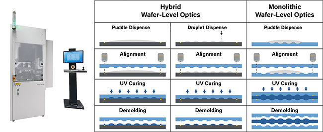
Figure 2. The EVG IQ Aligner, a versatile system for precision alignment and fully recipe-controlled lens molding,
is depicted together with common
process flows used by the industry. Courtesy of EV Group.
In wafer-level optics manufacturing, it is important to distinguish between hybrid glass-polymer and fully monolithic polymer components, since each has unique process requirements and advantages. Hybrid lenses, which utilize glass substrates, are most commonly used by optics manufacturers today. The formation of hybrid lenses is facilitated by the rigid nature of the glass substrates, which allows the lenses to rely on substrate-handling concepts that have been well proved in mature semiconductor manufacturing lines, such as robot end effectors and cassettes. Additionally, it makes the final products more reliable and less sensitive to temperature variations.
Monolithic lenses are made entirely of UV curing polymers and have the key advantage that the top and bottom lenses can be fabricated in a single step, as depicted in Figure 2. Furthermore, without the glass substrate as a carrier for the lenses, it allows the manufacture of even thinner devices.
For most micro-optics today, the typical height of such lenses is in the range of a few tens of microns up to hundreds of microns. Thus, the polymer has to be dispensed by either a puddle or a droplet. Whereas the puddle can be easily applied in a single step in the wafer center or bottom stamp and is squeezed to the edge during molding, the droplet dispense approach places the polymer sequentially only in the specified areas. Both methods will show comparable results for the actual lens quality because the substrate typically has no optical functionality; consequently, they differ mainly in terms of process integration.
The actual molding process starts with an alignment procedure using global alignment marks. This is necessary to ensure high-quality modules because the optical path is defined by the accuracy of the positioning of the lenses and other optical components in relation to each other. The actual molding process is performed in ambient conditions with gap- or force-controlled contact and UV curing. Equipment and process performance in this step are crucial for the replication fidelity and the uniformity of the lenses.
Success of replication
After the material is solidified, the stamp is demolded and reused for the next wafer. The demolding performance and the according automation is key for scaling the process to high volume. This aspect is not only controlled by the equipment but is closely related to process control and working know-how regarding stamp materials.
In production mode, the wafer-level molding process is key for achieving a high number of yielding products. And it is even more important to control the master stamp and working stamp quality. As for any replication process, preform defines the final result that makes the stamp manufacturing technology an integral part of successful manufacturing.
First, a wafer-level master has to be set up with equally high performance and quality of all lenses on the wafer. Creating the wafer-level master is typically done by step-and-repeat (S&R) imprinting. In this way, a high-quality single lens or a microlens array can be scaled to any given wafer size.
Because this mastering process is more time-consuming than replicating a whole wafer, the industry established the use of working stamps rather than imprinting with the actual master. In this way, risk mitigation and yield management can be optimized because working stamps can be renewed and replicated much more easily than master stamps. Additionally, the polarity of the master and the imprint are similar, which helps to qualify the pattern fidelity using profilometry — the extraction of topographical data from a surface — or 3D microscopy. This results in the working stamp becoming the actual link between the master and the product.
For many years, the working stamp was a challenge for high-volume manufacturing, and polydimethylsiloxane (PDMS)-based materials could be scaled only with substantial effort due to long process times and limited accuracy in shape because of swelling effects. In recent years, new materials for working stamps have been used that enable highly accurate replication with high-
volume manufacturing (HVM)-compatible process conditions. These new working stamps can be manufactured within minutes to enable controlled low-force demolding and are not prone to swelling.
As depicted in Figure 3, the pattern fidelity of the lens is preserved at each step in the replication process, from S&R lens master to working stamp to actual imprint.
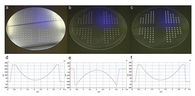
Figure 3. Lens wafers starting from S&R master (a) and working stamp (b) to final imprint (c). All lenses show a smooth surface and high
uniformity, verified using a profilometer (d-f). Courtesy of EV Group.
To qualify the performance of decisive process steps, infrastructure has been established that enables the development of manufacturing-ready solutions. This efficiency is possible due to the scaling of lens molding and nanoimprint lithography from a single lens — or respectively, a single die — up to the wafer level, and to the implementation of fully automated system integration. As an example, the EV Group’s NILPhotonics Competence Center (Figure 4) is an open-access innovation incubator.
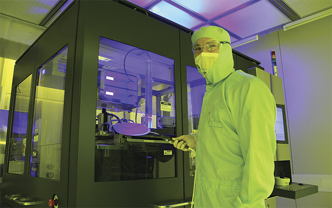
Figure 4. The NILPhotonics Competence Center is an open-access innovation incubator for nanoimprint lithography, providing S&R mastering services for wafer-level optics. Courtesy of EV Group.
Future of wafer-level optics
Many good ideas fail to make it to market because they miss the opportunity to prove that a single prototype can be scaled to necessary volumes. Very often, single lenses, microlens arrays, diffractive optics, nanogratings, diffusors, beamsplitters, and homogenizers are designed or even available at the die level but are too costly to produce on larger areas.
This gap is bridged by the S&R mastering technology3, which enables production scaling from small dies up to full wafer-scale masters. These master stamps are fully populated with microlens molds, each replicated from a single lens or lens array template in an S&R approach. The integration of small-form photonic sensors supports the industry’s need to find new schemes for prototyping and process development, which can keep pace with the speed of the market.
Meet the authors
Martin Eibelhuber, Ph.D., is deputy head of business development at EV Group, overseeing bonding, lithography, and nanofabrication technologies, with a particular focus on compound semiconductors, nanotechnology, and photonics applications. He has a doctorate in technical physics from the Johannes Kepler University Linz, specializing in nanoscience and semiconductor physics.
Robert Breyer is head of process technology for large-area/lens/S&R nanoimprint lithography at EV Group. He has an educational background in material engineering (HTL Andorf, Upper Austria). Breyer is responsible for customer and development projects for wafer-level optics, lens molding, and panel-size nanoimprinting for display applications. Additionally, he supervises the S&R mastering services within EVG’s NILPhotonics Competence Center.
Mikhail Begel is process engineer at EV Group. He received an M.Sc. degree in nanotechnology from Friedrich-Alexander University Erlangen in Germany. Begel is involved in supporting presales activities through customer-specific sample processing and demonstration of processes on the equipment. He is responsible for process development and support in micro- and nanoimprint lithography, especially for wafer-level optics and lens molding applications.
References
1. H. Han et al. (2010). Wafer level camera technology — from wafer level packaging to wafer level integration. Presented at 11th International Conference on Electronic Packaging Technology & High Density Packaging.
2. M. Eibelhuber et al. (Feb. 2015). Nanoimprint Lithography enables cost-effective photonics production. Photonics Spectra, Vol. 49, Issue 2, pp. 34-37.
3. G. Kreindl et al. (2010). High accuracy UV-nanoimprint lithography step-and-repeat master stamp fabrication for wafer level camera application. J Vac Sci Technol B, Vol. 28, C6M57.