Engineers from Vanderbilt University developed a method of simultaneously transmitting two types of optical signals across a single chip. The work may enable a dramatic increases in the volume of data a silicon chip can transmit over any period of time, directly supporting “lab-on-a-chip” capabilities.
Engineers design waveguides to work at a single frequency of light, typically 1550 nm, Joshua Caldwell, associate professor in Vanderbilt’s Department of Mechanical Engineering, told Photonics Media. The number of waveguide channels, limited by the amount of space on a chip, defines the number of signals a chip is able to process.
“Frequency multiplexing is a concept where you can simultaneously process two different signals at two different frequencies,” Caldwell said.
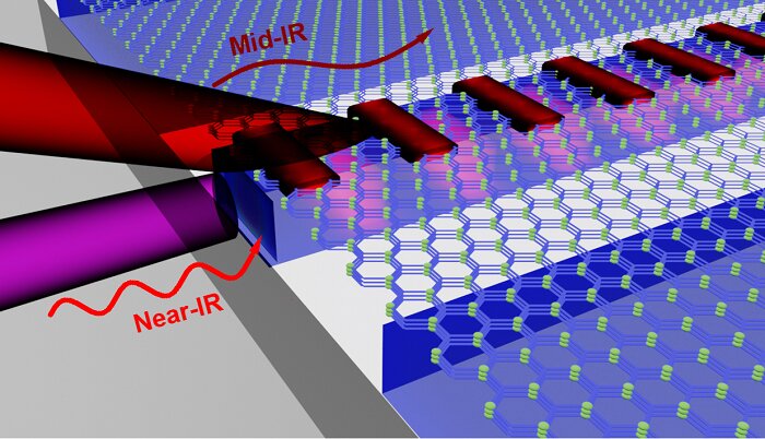
Researchers devised a hybrid, hyperbolic-silicon photonic waveguide platform that transmits mid-IR and near-IR light at the same time, on the same chip, demonstrating dual-band optical processing. Courtesy of Caldwell Lab, Vanderbilt University.
The problem with the concept is that it requires a second waveguide with a different width to work at the other frequency. Just like doubling the the number of channels, incorporating that requirement takes up space. Further, linear scaling, for the purpose of accommodating an increased number of waveguides, would quickly surpass the amount of available space on a silicon chip in the standard form factor.
“It has been difficult to combine near-infrared and mid-infrared in the same device,” said Mingze He, first author on the paper and a Ph.D. student in mechanical engineering at Vanderbilt.
The method developed by Caldwell and his team added a path to incorporate another frequency without taking up much more real estate. “Our approach provides a second ‘waveguide’ using a layer of hexagonal boron nitride,” Caldwell said.
Hexagonal boron nitride (hBN) is able to transmit light at long waves from 6200 to 7300 nm in very thin slabs. The researchers used a 237-nm slab, though that size isn’t a limit, Caldwell said.
“The difference in the refractive index underneath the boron nitride layer between the silicon waveguide and the surrounding air ensures the light in the boron nitride will follow the same path of the silicon,” he said.
The hybrid hyperbolic-silicon photonic waveguide leverages the optical properties of both materials. In the mid-IF, the hBN crustal is able to support an optical mode called a hyperbolic phonon polariton, which is generated through light coupling with the polar bonds in the crystal. This allowed the long-wavelength mid-IR to be focused and transmitted within deeply subwavelength structures and slabs.
The light is compressed well below the free-space wavelength, in this case 6200 to 7300, so that they are compatible with the same silicon photonics platforms used in the near-IF. Generating those modes requires a diffraction grating, a prism, or a very small object scattering light.
“Here we used the atomic-force microscope tip used within our scattering-type scanning near-field optical microscope that we used for this study,” Caldwell said. “In a real device, you would probably use some type of in-coupler like a patterned grating to achieve this.”
The work enables the use of multiple frequencies simultaneously in optical processing, but specifically, Caldwell said, it would allow the boron nitride mid-IR channel to be used for tasks such as chemical sensing, with the signal in the silicon waveguides used to transmit that information within the device.
“There are a variety of opportunities this raises, but in this vein this could be impactful for technologies such as the so-called lab-on-a-chip,” Caldwell said.
Currently, the team has new work under review, focused on using these materials for label-free nanoscale imaging concepts and integration with photonic crystals.
The research was published in Advanced Materials (www.doi.org/10.1002/adma.202004305).